动态加载课题
随便写写
1 | |
1 | |
iic
- MYIR-ZYNQ7000系列-zturn教程(22):用axi_iic对24C32进行读写https://blog.csdn.net/taowei1314520/article/details/85232219
bugs
vitis
1) microblaze直接run as程序出错:no targets found with “name = ~ “microblaze#0” & bscan
microblaze没有JTAG接口
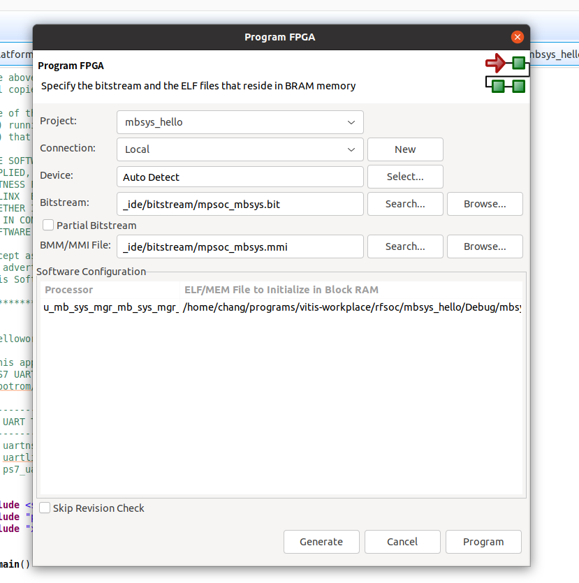
2) 如何正确运行mb程序(基于HTG-ZRF8)
步骤:
- 导出xsa
- Vitis Create Platform(如果直接Create App会导致之后再在该Workplace中添加app project时找不到platform)
- 编译platform
- create mb程序并编译
- program FPGA,并把mb程序替换为上面mb project生成的elf文件
- program FPGA后就会出现hello world
补充,使用jtag进行mb调试的步骤:
- 导出xsa
- Vitis Create Platform(如果直接Create App会导致之后再在该Workplace中添加app project时找不到platform)
- 编译platform
- create mb程序并编译
- program FPGA,并把mb程序替换为上面mb project生成的elf文件
- 这一步进行比特流加载
- 右键mb project,run as hardware
- 这一步进行程序烧录
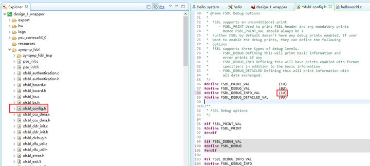
3) fsbl
修改调试宏定义FSBL_DEBUG_INFO_VAL,可以在启动输出FSBL的一些状态信息,有利于调试,但是会导致启动时间变长。保存文件。可以看一下fsbl里包含了很多外设的文件,包括psu_init.c,qspi,sd等,大家可以再仔细读读代码。当然这个fsbl模板也是可以修改的,至于怎么修改根据自己的需求来做
4) Zynq UltraScale+ MPSoC Software Developer Guide
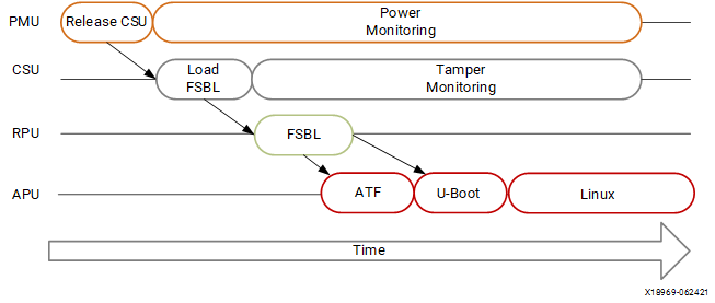
Boot Flow
There are two boot flows in the Zynq UltraScale+ MPSoC architecture: secure and non-secure. The following sections describe some of the example boot sequences in which you bring up various processors and execute the required boot tasks.
Note: The figures in these sections show the complete boot flow, including all mandatory and optional components.
Boot Flow Example
The QSPI boot mode supports the following:
QSPI 启动模式支持以下内容:
x1, x2, and x4 read modes for single Quad SPI flash memory (QSPI24) and x8 for dual QSPI
Image search for MultiBoot
I/O mode is not supported in FSBL
The SD boot supported version is 3.0. This version supports:
- FAT 16/32 file systems for reading the boot images.
- Image search for MultiBoot. The maximum number of searchable files as part of an image search for MultiBoot is 8,191.
For additional information, see SD Boot Mode.
https://docs.xilinx.com/r/en-US/ug1137-zynq-ultrascale-mpsoc-swdev/SD-Boot-Mode
5) Xilinx Embedded-Design-Tutorials
Boot Sequence for SD-Boot
6)sd-ls
SD1(LS): The SD1-LS boot mode is the same as SD0/SD1 with additional support of the SD 3.0 (with an SD 3.0 compliant voltage level shifter).
sdio_cd_n
Card detection for single slot
7)Flash
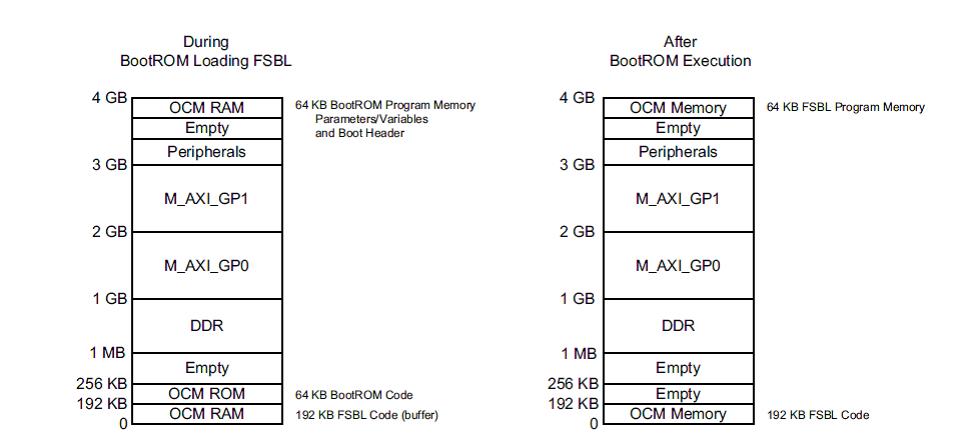
FSBL Build Process
After authenticating and/or decrypting, the FSBL is loaded into OCM and handed off by the CSU bootROM. First Stage Boot Loader configures the FPGA with a bitstream (if it exists) and loads the Standalone (SA) Image or Second Stage Boot Loader image from the non-volatile memory (NAND/SD/eMMC/QSPI) to RAM(DDR/TCM/OCM). It takes the Cortex-R5F-0/R5F-1 processor or the Cortex-A53 processor unit out of reset. It supports multiple partitions. Each partition can be a code image or a bitstream. Each of these partitions, if required, will be authenticated and/or decrypted.
Note: If you are creating a custom FSBL, you should be aware that the OCM size is 256 KB and is available to CSU bootROM. The FSBL size is close to 170 KB and it would fit in the OCM. While using the USB boot mode, you should make sure that the PMU firmware is loaded by the FSBL and not by the CSU bootROM. This is because the size of boot.bin loaded by the CSU bootROM should be less than 256 KB.
在验证和/或解密之后,FSBL 被加载到 OCM 中,并由 CSU 引导 ROM 传递。第一阶段引导加载程序将 FPGA 配置为一个比特流(如果存在的话) ,并将独立(SA)映像或第二阶段引导加载程序映像从非挥发性记忆体(nAND/SD/eMMC/QSPI)加载到 RAM (DDR/TCM/OCM)。它取消了 Cortex-R5F-0/R5F-1处理器或 Cortex-A53处理器单元的重置。它支持多个分区。每个分区可以是代码图像或位流。如果需要,这些分区中的每一个都将进行身份验证和/或解密。
注意: 如果您正在创建一个自定义 FSBL,您应该知道 OCM 大小是256 KB,并且可用于 CSU 引导 ROM。FSBL 的大小接近170 KB,它将适合在 OCM。在使用 USB 引导模式时,您应该确保 PMU 固件是由 FSBL 加载的,而不是由 CSU 引导 ROM 加载的。这是因为 CSU bootROM 加载的 boot.bin 的大小应该小于256 KB。
https://docs.xilinx.com/r/en-US/ug1137-zynq-ultrascale-mpsoc-swdev/Fallback-and-MultiBoot-Flow
1.3 Memory Map, Boot flow and Reference Applications
This tech-tip describes the Boot flow of Zynq -7000 series platforms and provide details on application pre-loading in to L2 cache, locking it, and executing application out of L2 cache. It covers both C, and Cpp based application for demonstration.
QSPI Flash Memory Map:
Quad-SPI linear address space of 16MB with address range FC00_0000 to FDFF_FFFF. Which can be used for execute in place option (XIP). FSBL uses this option in the reference design to execute the FSBL.
OCM Memory Map:
Zynq-7000 series platform has On-chip memory of 256KB, default address range at 0000_0000 to 0003_FFFF of 192kB and FFFC_0000 to FFFF_FFFF of 64KB.
本博客所有文章除特别声明外,均采用 CC BY-SA 4.0 协议 ,转载请注明出处!