静态时序分析
静态时序分析
- 讲义下载:https://customizablecomputinglab.gitee.io/2020/08/07/class-STA/
- 课程网站:https://www.bilibili.com/video/BV1if4y1p7Dq
参考阅读
0 目录
- 1 静态时序分析课程概述
- 2 TCL
- 3 Synopsys TCL语言入门
- 4 STA基本概念
- 5 标准单元库
- 6 STA环境配置(重要)
- 7 Timing Verification(一) 时序检查
- 8 Timing Verification(二) 多周期半周期伪路径检查
- 9 Timing Verification(三) 多时钟域,多时钟分析
- 10 Robust Verification鲁棒性检查
- 11 Time Borrowing/Cycle Stealing
- 12 Data to Data Checks
- 13 习题讲解
1 静态时序分析课程概述
- 数字芯片与FPGA设计流程
- 静态时序分析概述
- 课程内容规划
1.1 数字芯片与FPGA设计流程
1)数字芯片设计流程
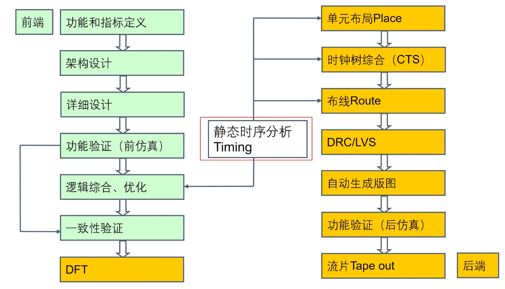
- 数字前端
- 功能验证(前仿真):逻辑功能的仿真
- 1~4步(功能验证)和实际的工艺库没有强依赖关系
- 逻辑综合、优化:加入工艺库
- 一致性验证:netlist和rtl design进行比较
- 数字后端
- DRC/LVS:生成版图
- 功能验证(后仿真):时序仿真
2)FPGA设计流程
- 综合
- 综合后得到netlist,此netlist未在fpga上规划坐标
- 实现
- 布局
- 布线
fpga设计也要求加入约束完成静态时序分析
1.2 静态时序分析概述
1)核心两点
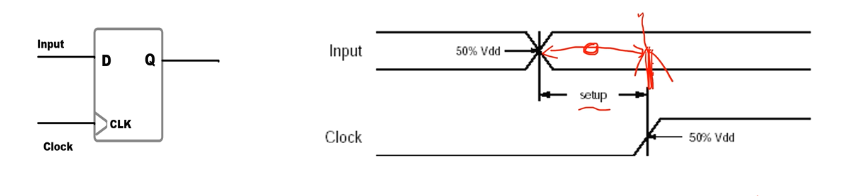
Setup Time :采样的D触发器的时钟上升沿之前,数据稳定下来的时间(保证采样稳定)
Setup Time 建立时间 -The length of time that data must stabilize before the clock transition.
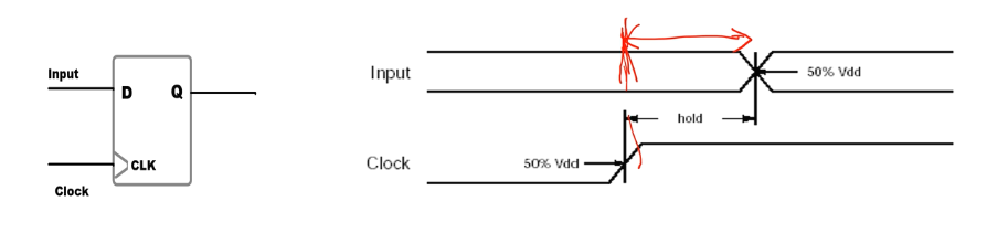
Hold Time:采样的D触发器的时钟上升沿之后,数据依然保持稳定的时间(如果不稳定,造成数据传输错误)
Hold Time保持时间:The length of time that data must remain stable at the input pin after the active clock transition.
静态时序分析的内容:
静态时序分析最核心的两点就是检查setup和hold,来确认每一个触发器的工作是否能正确采集数据
- 对于同步电路需满足每一个触发器的setup和hold
- 补充:大部分EDA
- 对于异步电路不一样,其指标不同
- 补充:异步电路单独拿出来处理,通常需要单独重点处理
- 实际上当下soc复杂,可以看作全局异步局部同步的电路
- 局部模块中使用STA的方法分析setup\hold
- 整体时考虑每个时钟域下,数据传递的样态、怎么降低样态出现的概率
2)静态时序分析所在阶段
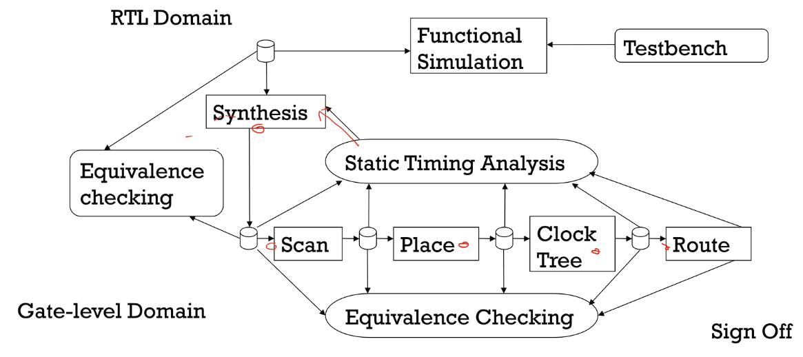
Synthesis、Scan、Place、ClockTree、Route,每一个区域中的STA模型略有区别
3)功能验证与STA的大体区别
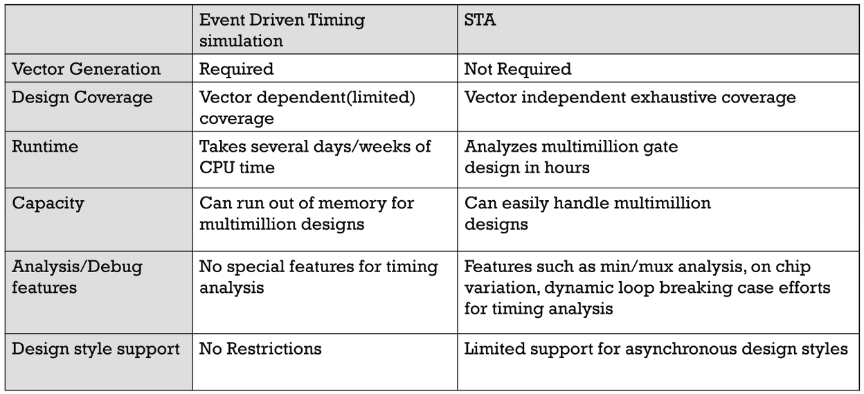
保持功能正常的两种手段:simulation、sta
simulation:不同的生成各种测试向量确保功能覆盖率
- 仿真太慢,很多公司使用emulator来加速
sta:确认每一个触发器的setup,hold是否能正确地采样,不关心功能,不需要设计测试向量
- 优点:相对简单,不需要穷举性的测试向量;耗时短,快速
- 可能的场景:当没有把握测试到所有功能,可以使用sta进行补充
1.3 课程主要内容
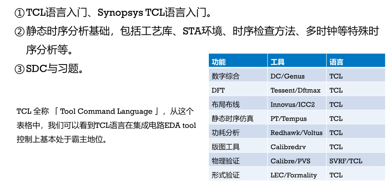
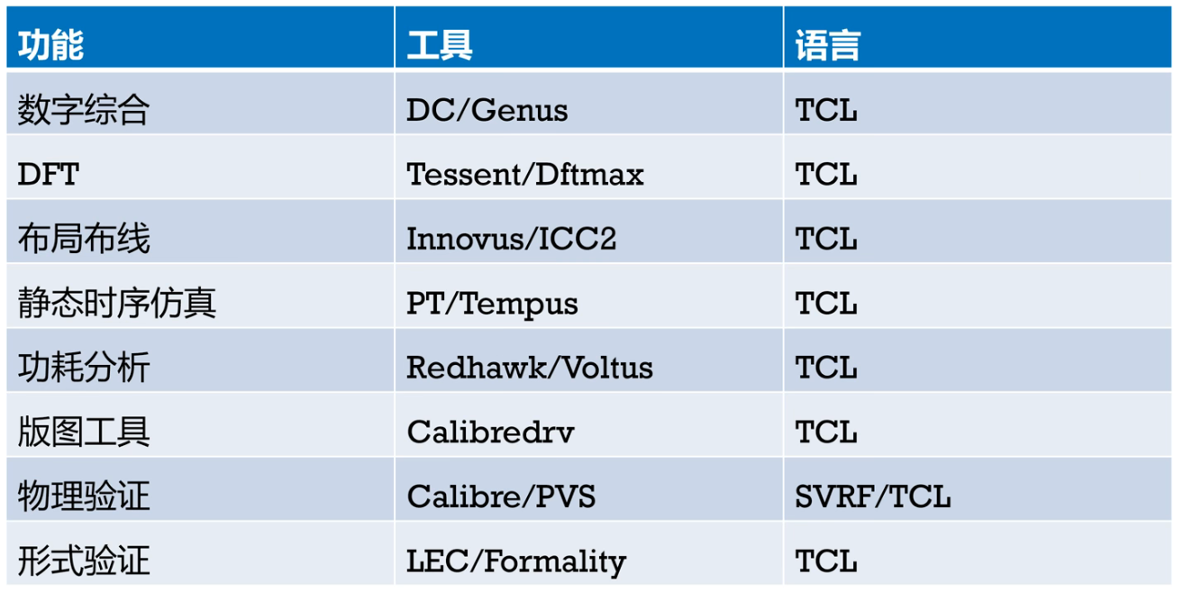
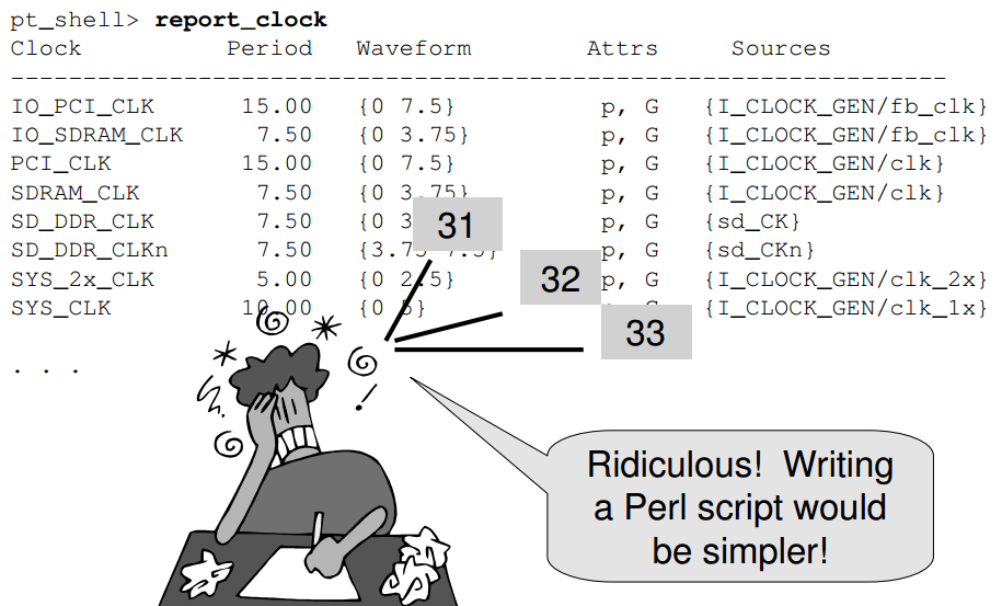
STA工具用的最多的:synopsys的Pertime(PT),每个EDA公司都有自己的静态时序分析工具,每个功能处(数字综合、DFT、布局布线)其实也都嵌入了PT引擎
参考图书:
①《Static Timing Analysis for Nanometer Designs:A Practical Approach》J.4Bhasker,Rakesh Chadha.Springer Science Business Media,LLC 2009.
- 非常经典,课程教材,希望精读,专讲静态时序机理
②《综合与时序分析的设计约束:Synopsys设计约束(SDC)实用指南》[美]斯里达尔·甘加达兰(Sridhar Gangadharan),[印度]桑杰·丘里瓦拉(Sanjay,Chur著,韩德强张丽艳王宗侠等译译.出版社:机械工业出版社出版时间:2016-06-01.
- 感兴趣可以看
③《集成电路静态时序分析与建模》.刘峰,机械工业出版社.出版时间:2016-07-01.
- 国内写的,tcl脚本讲的好,可以补充12本的知识
④《Using Tcl with Synopsys Tools.Version B-2008.09》March 2011.Synopsys.
- Synopsys的tcl手册
2 TCL
- 概述
- 变量、数组、列表
- 控制流
- 过程函数
- 正则匹配(重要)
- 文本处理
2.1 概述
1)TCL
TCL在EDA工具中非常重要
不同语言的区别

- shell原生兼容性较好
- tcl整个eda工具的标准语言
- per更像转接头,eda工具无法原生支持,使用tcl操作eda工具,外层使用perl处理文本控制字符串
- python近些年用的多一些
2)如何使用tcl
Linux系统下
- 输入
tclsh - 在文本第一行
#!/user/bin/tclsh(TCL的安装路径)
Windows系统下
- 安装active tcl并双击wish.exe
2.2 置换机制
TCL解释器运用规则把命令分成一个个独立的单词,同时进行必要的置换
TCL置换分为以下三类:
- 变量置换$
- 命令置换[]
- 反斜杠置换\
- C语言常用
1)变量置换
用$表示变量置换
- TCL解释器会将认为$后面为变量名,将变量置换成它的值
2)命令置换
用[]表示命令置换
- []内是一个独立的TCL语句

3)反斜杠置换
用\表示反斜杠置换
- 换行符、空格、[、$等被TCL解释器当作特殊符号对待的字符,加上反斜杠后变成普通字符
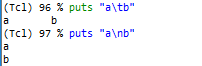
4)其他符号
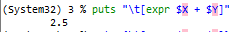
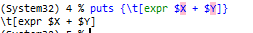
双引号”” TCL解释器对双引号中$和[]符号会进行变量置换和命令置换
花括号{} 花括号中所有特殊字符都将成为普通字符,TCL解释器不会对其作特殊处理。
#表示注释

2.3 变量、数组、列表
1)变量
定义:set 变量名 变量值
取值:$变量名
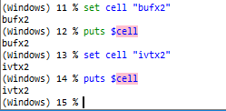
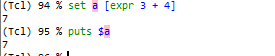
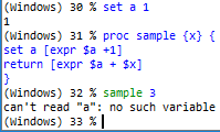
- 例题:假设我们想打印变量varible,后面跟一个”_1”,会发生什么呢?
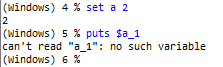
直接写a_1会造成引用

使用{}置换做限定
2)数组
数组: TCL中数组可以存储很多值,通过元素名来进行检索。类似于某件事物(数组名)几种不同属性(元素名),每一种属性有其独立的值
定义: set 数组名(元素名) 值
- 取值: $数组名(元素名)

- 使用array指令获取数组信息

3)列表(重要的数据结构)
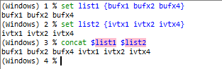
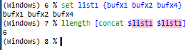
- 列表是标量的有序集合。
- 定义 set 列表名 {元素1 元素2 元素3……}
- 取值 $列表名
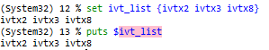
TCL中有一系列十分方便的列表操作命令

列表指令-concat
- 语法格式 : concat 列表1 列表2
- 功能: 将列表1和列表2合并 (设计中很常用,比如合并两个时钟组放在一起)
列表指令-llength
语法格式 : llength 列表
功能:返回列表中的元素个数
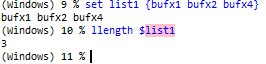
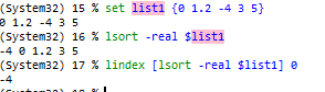
- 例题: list1为{bufx1 bufx2 bufx4},那么 llength [concat $list1 $list1] 会得到多少呢?
- 列表指令-lindex
- 语法格式 : lindex 列表 n
- 返回列表中第n个元素(从0开始计数)
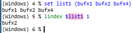
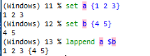
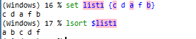
- 如何得到列表list1 {a b c d e f}的最后一个元素?
列表指令-lappend
- 语法格式 : lappend 列表 新元素
- 功能: 列表末尾加入新元素

- 例题:如果我们lappend一个列表会怎么样?
- 如果我们想得到4 用什么样的命令?
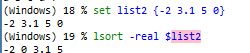
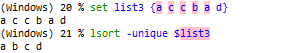
列表指令-lsort
- 语法格式 : lsort 开关 列表
- 功能: 将列表按照一定规则排序
- 开关: 缺省时默认按照ASCII码进行排序。
- –real 按照浮点数值大小排序
- -unique唯一化,删除重复元素
- 按照ASICC码排序
- 按照数字大小排序
- 唯一化
- 例题:如何得到列表list1 {0 1.2 -4 3 5}中的最小值?


2.4 运算
数学运算:+,-,*,/
逻辑运算:<=,>=,==,!=
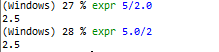
1)数学运算指令-expr
- 语法格式 : expr 运算表达式
- 功能: 将运算表达式求值
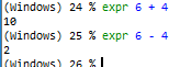
- 例题:我们在TCL中经常会遇到下面的现象
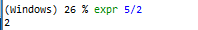
- 其原因是表达式5/2中5和2都是整数型参数, 默认运算结果也是整数型。如果想要进行浮点运算, 只要将其中任意一个数值, 写成浮点形式(有小数点) 即可
2.5 控制流
1)控制流-if
- 语法格式:注意括号一定要在一行里面,不能在下一行
- 注意,下例中脚本语句的’{‘一定要写在上一行,因为如果不这样, TCL 解释
器会认为if命令在换行符处已结束,下一行会被当成新的命令,从而导致错误
1 | |
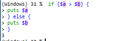
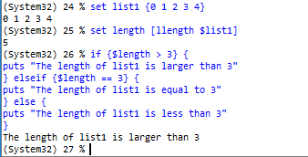
- 例题:我们如何判断一个列表{0 1 2 3 4}的长度是大于3,还是等3,还是小于3?
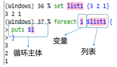
2)循环指令-foreach
语法格式 : foreach 变量 列表 循环主体
- 与C语言for不一样,在tcl里面很强大
功能:从第0个元素开始, 每次按顺序取得列表的一个元素, 将其赋值给变量, 然后执行循环主体一次, 直到列表最后一个元素

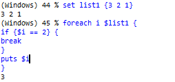
3)循环控制指令-break
- 语法格式 : break
- 功能: 结束整个循环过程,并从循环中跳出
4)循环控制指令-continue
- 语法格式 : continue
- 功能: 仅结束本次循环
5)循环控制指令-while
- 语法格式 : while 判断语句 循环主体
- 功能: 如果判断语句成立(返回值非0),就运行脚本,直到不满足判断条件停止循环,此时while命令中断并返回一个空字符串。
6)循环控制指令-for
语法格式 :
for 参数初始化 判断语句 重新初始化参数 循环主体功能: 如果判断语句返回值非0就进入循环,执行循环主体后,再重新初始化参数。然后再次进行判断,直到判断语句返回值为0,循环结束。
2.6 过程函数
1)过程函数-proc
- 语法格式 : proc 函数名 参数列表 函数主体
- 功能: 类似于C语言中的函数。即用户自定义的功能,方便多次调用。
2)全局变量与局部变量
- 全局变量:在所有过程之外定义的变量。
- 局部变量:对于在过程中定义的变量,因为它们只能在过程中被访问,并且当过程退出时会被自动删除。
- 指令global,可以在过程内部引用全部变量
使用global引用

不使用gloabl引用,导致出错
2.6 正则匹配
1)正则匹配
定义:正则表达式是一种特殊的字符串模式,用来去匹配符合规则的字符串。
正则表达式的\w,用来匹配一个字母、数字、下划线
正则表达式的\d ,用来匹配一个数字
1 | |
2)正则匹配-量词
- \w\w\w\d\d\d这种写法过于繁琐,我们可以用代替重复的量词进行表示 ,在TCL中常用一下三种量词
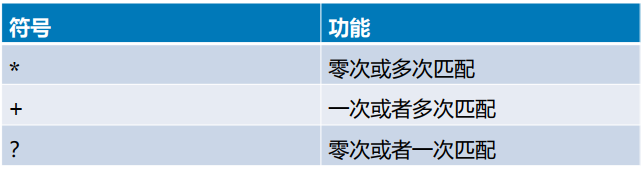
1 | |
- 和+的区别: 可以是零次, +一个至少是一次
1 | |
- ?表示零次或者一次匹配
1 | |
3)正则匹配-锚位
锚位,用来指示字符串当中的开头和结尾的位置,使我们能够匹配到正确的字符


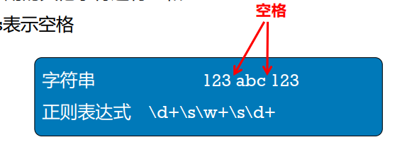
4)正则匹配-其他字符
- 常用的其他字符还有\s和.
- \s表示空格
- . 表示任意一个字符
- 我们不确定具体是什么字符是就可以用.表示。例如已知知字符串为”xxx空格xxx空格xxx”(x为未知字符)。用.+\s.+\s.+就可以匹配
5)正则匹配指令-regexp
语法格式 : regexp? switches? exp string? matchVar? ?subMatchVar subMatchVar …?
功能: 在字符串中使用正则表达式匹配
- switches:
- -nocase将字符串中的大写都当成小写看待。
- exp 正则表达式
- string 用来进行匹配的字符串
- matchstring表示用正则表示式匹配的所有字符串
- sub1表示正则表达式中的第一个子表达式匹配的字符串
- sub2表示正则表达式中的第二个子表达式匹配的字符串
- switches:
例题:
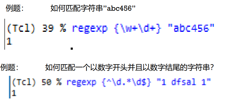
6)捕获变量
- 通过()可以捕获字符串
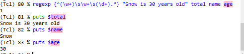
- 例如如何将字符串“Snow is 30 years old”中30捕获出来?
- 例如如何将字符串“Snow is 30 years old”中30捕获出来?
- 一次捕获多个字符串(多加几个变量)
- 例如如何将字符串“Snow is 30 years old”中Snow 和30一次捕获?
- 例如如何将字符串“Snow is 30 years old”中Snow 和30一次捕获?

2.7 文本处理
用TCL处理文本在工作中十分常用,主要掌握以下三个指令:
- get
- gets
- close
gets
- 语法格式 gets fileId 变量名
- 功能 gets读fileId标识的文件的下一行,并把该行赋给变量,并返回该行的字符数(文件尾返回-1)
open
- 语法格式 open 文件 打开方式(打开方式 r表示读模式, w表示写模式。)
- 功能 打开文件
close
- 语法格式 close fileid
- 功能 关闭文件
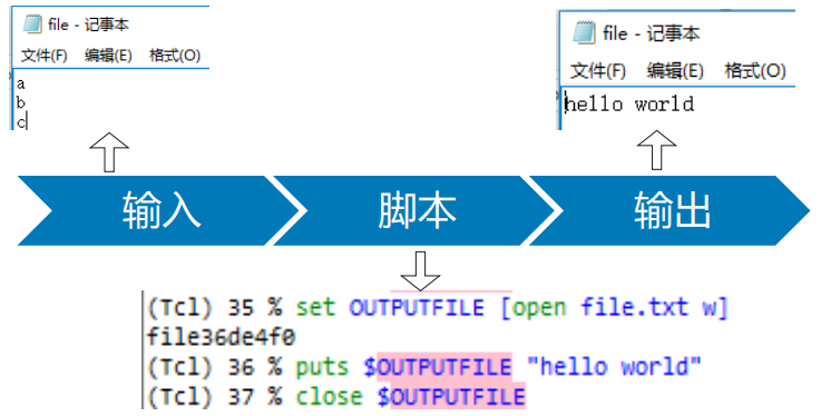
例题: 整个读入文件过程 :

例题:一个完整写入文件过程
例题:现有文本file.txt其内容如下。请写一TCL脚本求出所有Slack值之和
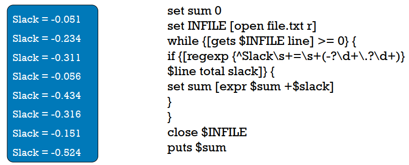
- 使用正则匹配Slack = -
2.8 参考书
- 《Using Tcl with Synopsys Tools》. Version B-2008.09, March 2011. Synopsys.
- 《集成电路静态时序分析与建模》. 刘峰, 机械工业出版社.出版时间: 2016-07-01
3 Synopsys TCL语言入门
- TCL在EDA工具中的扩展与应用
- 使用TCL控制EDA工具流程
3.1 TCL的应用
1)Overview

内建命令
应用命令
用户自定义命令
2)Why Synopysy TCL
数时钟
使用TCL更简单

SynopsysTCL扩展命令参考资料:
- Using Tcl with SynopsysTools
- PrimeTime User Guide: Fundamentals:
- PrimeTime User Guide: Advanced Timing Analysis
3.2 TCL在EDA工具中的扩展与应用
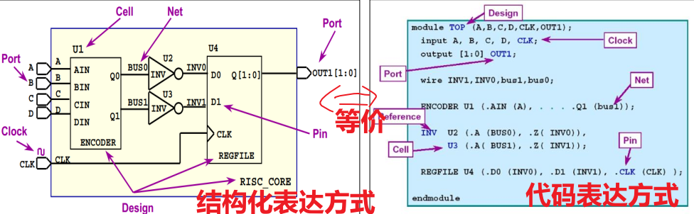
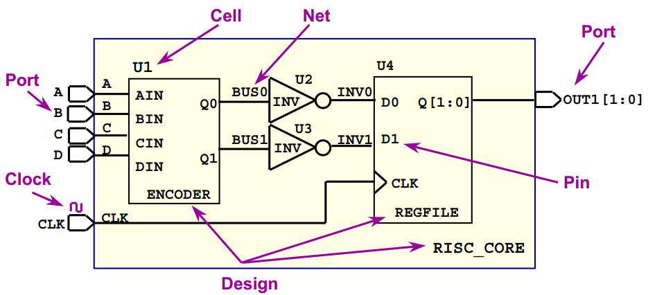
1)TCL的应用:Design Object
通过对Design Object的分析,我们来了解和学习DC获取电路并进行解析的方法
- 指令都在DC环境中输入,可以在GUI界面下方窗口,也可以在DC命令行
- DC里面net是一种collection
- ref与inst
- reference是module
- inst是实例化的module
2)综合软件当中TCL的常见指令(SynopsysTCL扩展的指令)
(1)获取对象
获取port object
- 语法格式: get_ports portsName
- 指令功能:返回design中对应的ports object
例-1:如何查看design当中有没有一个port叫做CLK?
- Shell> get_ports CLK
{CLK}
- Shell> get_ports CLK
例-2:我们想查看design当中有没有一个port叫做SPI?
- Shell> get_ports SPI
No object Found!
- Shell> get_ports SPI
例-3:我们想查看design当中所有的port (*可以通配任何字符)
- Shell> get_ports *
{A B C D CLK OUT[0] OUT[1]}
- Shell> get_ports *
- 例-4:假设我们有port名字叫 {CLKA CLKB OUTA OUTB INA INB}
如果我们想得到所有C开头的port 怎么做?- Shell> get_ports C*
{CLKA CLKB}
- Shell> get_ports C*
获取cell object
- 语法格式: get_cells cellsName
- 指令功能:返回design中对应的cell的instance name object
- 举例-1:我们想查看design当中有没有一个cell叫做U4?
- Shell> get_cells U4
{U4}
- Shell> get_cells U4
- 举例-2:我们想查看design当中所有的cell
- Shell> get_cells *
{U1 U2 U3 U4}
- Shell> get_cells *
- 举例-3:我们想查看design当中以3为结尾的cells
- Shell> get_cells *3
{U3}
- Shell> get_cells *3
获取net object
- 语法格式: get_nets netsName
- 指令功能:返回design中net的object
- 举例-1:查看design当中有没有一个net以INV开头?
- Shell> get_nets INV*
{INV0 INV1}
- Shell> get_nets INV*
- 举例-2:我们想查看design当中所有的nets
- Shell> get_nets *
{A B C D CLK BUS0 BUS1 INV0 INV1 OUT[0] OUT[1]
- Shell> get_nets *
- 举例-3:我们想查看design当中有多少个net?
- 方法1,TCL基本语法的写法:
Shell> llength [get_object_name [get_nets *]]
11 - 方法2,使用DC命令sizeof_collection获取:
Shell> sizeof_collection [get_nets *]
11 - 注意两条指令的区别噢!
- 方法1,TCL基本语法的写法:
获取pin object(引脚)
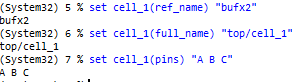
- 语法格式: get_pins pinsName
- 指令功能:返回design中pin的object
- 举例-1:查看design当中有哪些pin的名字叫做Z?
- Shell> get_pins */Z
{INV0/Z INV1/Z}
- Shell> get_pins */Z
- 举例-2:查看design当中有哪些pin的名字以Q开头?
- Shell> get_pins */Q*
{ENCODER/Q0 ENCODER/Q1 REGFILE/Q[1] REGFILE/Q[0]}
- Shell> get_pins */Q*
(2)“数据类型: object (对象) ”与其“属性”
object说明:
- object是对于tcl脚本一个重要的扩展;
- 常见的对象有四种 cell, net, port, pin;
- 每种object有它的属性。
- get_object_name
下面将介绍一些常见属性:
- 任何一个属性都可以用get_attribute得到,
- list_attribute –class * 可以得到所有object 的属性,
- 部分属性可以用set_attribute来设置
Cell object
- 属性 ref_name : 用来保存其map到的reference cell名称
- 例题:后端中常用于获取cell的ref
- Shell> get_attribute [get_cells –h U3] ref_name
{INV} 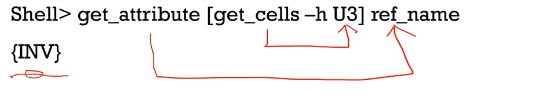
- Shell> get_attribute [get_cells –h U3] ref_name
Pin object
- 属性 owner_net : 用来保存与之相连的net的名称
- Shell> get_attribute [get_pins U2/A] owner_net
{BUS0} 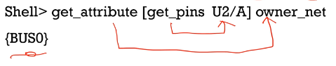
- Shell> get_attribute [get_pins U2/A] owner_net
Port object
属性 direction : 用来保存port 的方向
方法1
Shell> get_attribute [get_ports A] direction
{in}方法2,get_port OUT[i]
Shell> get_attribute [get_ports OUT[1]] direction
{out}
Net object:
- 属性 full_name : 用来保存net的名称
- Shell> get_attribute [get_nets INV0] full_name
{INV0} - Shell> get_object_name [get_nets INV0]
{INV0} - 一定需要通过[get_nets INV0]把net取出来
*Shell> get_attribute INV0 full_name
Error: No attribute found
- Shell> get_attribute [get_nets INV0] full_name
扩展get_* -f:
- 过滤属性
- get_ -f :
-f 这个option可以用来*过滤属性,以得到我们想要的object - 例子-1:想得到所有方向是input的port
- Shell> get_ports * –f “direction==in”
{A B C D CLK}
- Shell> get_ports * –f “direction==in”
- 例子-2:想得到所有方向是output的pin
- Shell>get_pins * -f “direction ==out”
{U1/Q0 U1/Q1 U2/Z U3/Z REGFILE/Q[0] REGFILE/Q[1]}
- Shell>get_pins * -f “direction ==out”
- 例子-3:想得到所有ref_name 是INV的 cell
- Shell>get_cells * -f “ref_name == INV”
{U2 U3}
- Shell>get_cells * -f “ref_name == INV”
扩展最关键的option -of:
- 获取连接的对象
- get_ [object]-of:
-of 这个option可以用来得到与你指定*object相连接的object - object的连接关系:
- —port object <-> net object
>get_nets –of [get_port A]
A - —net object <-> port object / pin object
> get_net –of [get_pin U2/A]
BUS0 - —pin object <-> net object
> get_pin -of [get_net INV1]
U3/Z - —cell object <-> pin object
>get_pins –of [get_cell U4]
{U4/D0 U4/D1 REGFILE/Q1 REGFILE/Q2}
- —port object <-> net object
自定义扩展TCL指令练习
- 得到电路中的所有inverter
- 解答:
- (1) 直接使用Synopsys TCL指令: get_buffers -inverter
- (2) 人工扩展TCL指令: get_inverters
人工扩展TCL指令: get_inverters
1 | |
3.3 使用TCL控制EDA工具流程
1)使用TCL语言设计DC的自动化Flow
内容:讲述一个简单的、入门级的Synopsys DesignComplier自动化方案,供初学者参考,感兴趣的同学对该方案进行优化和升级
特点:
- 该过程无需人为操作,用户只需要输入一条shell启动指令就能完全自动化的完成整个综合过程。
- 具备普适性和可重用性。在综合不同的设计时,只需要修改参数配置文件中的环境变量,不需要修
改脚本
思路:自动化电路综合平台只需用户将待综合的设计和库文件放入一个文件夹,修改与待综合设计对象有关的环境变量参数,在命令窗口唤醒DC的指令,即自动化地完成综合过程,并得到综合后的网表文件和所需的报告。

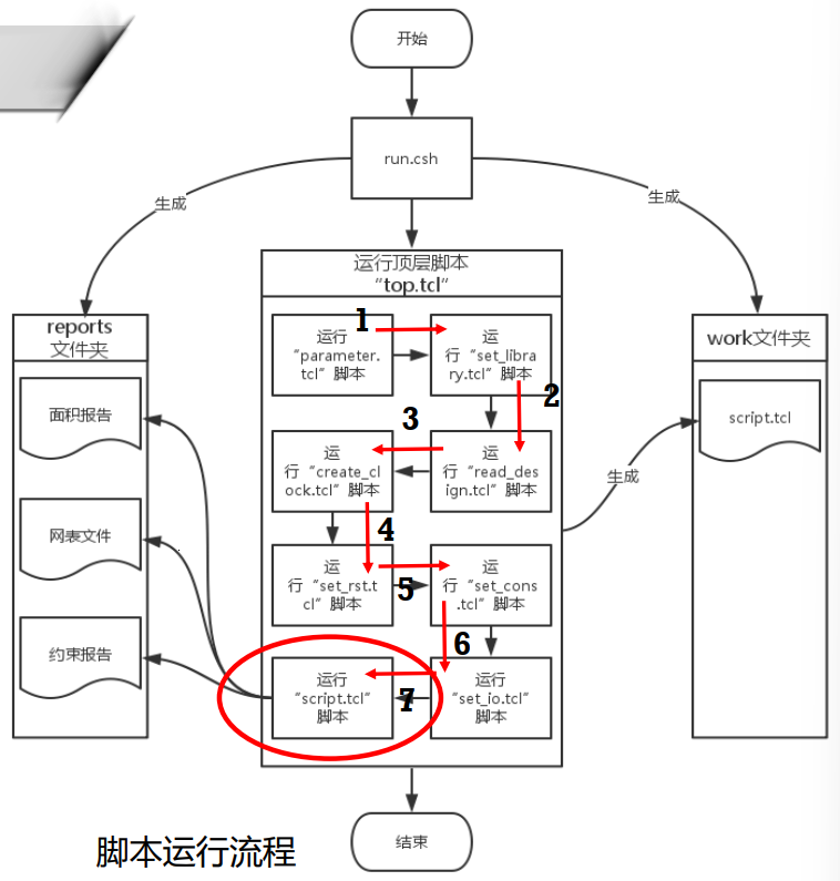
运行流程:
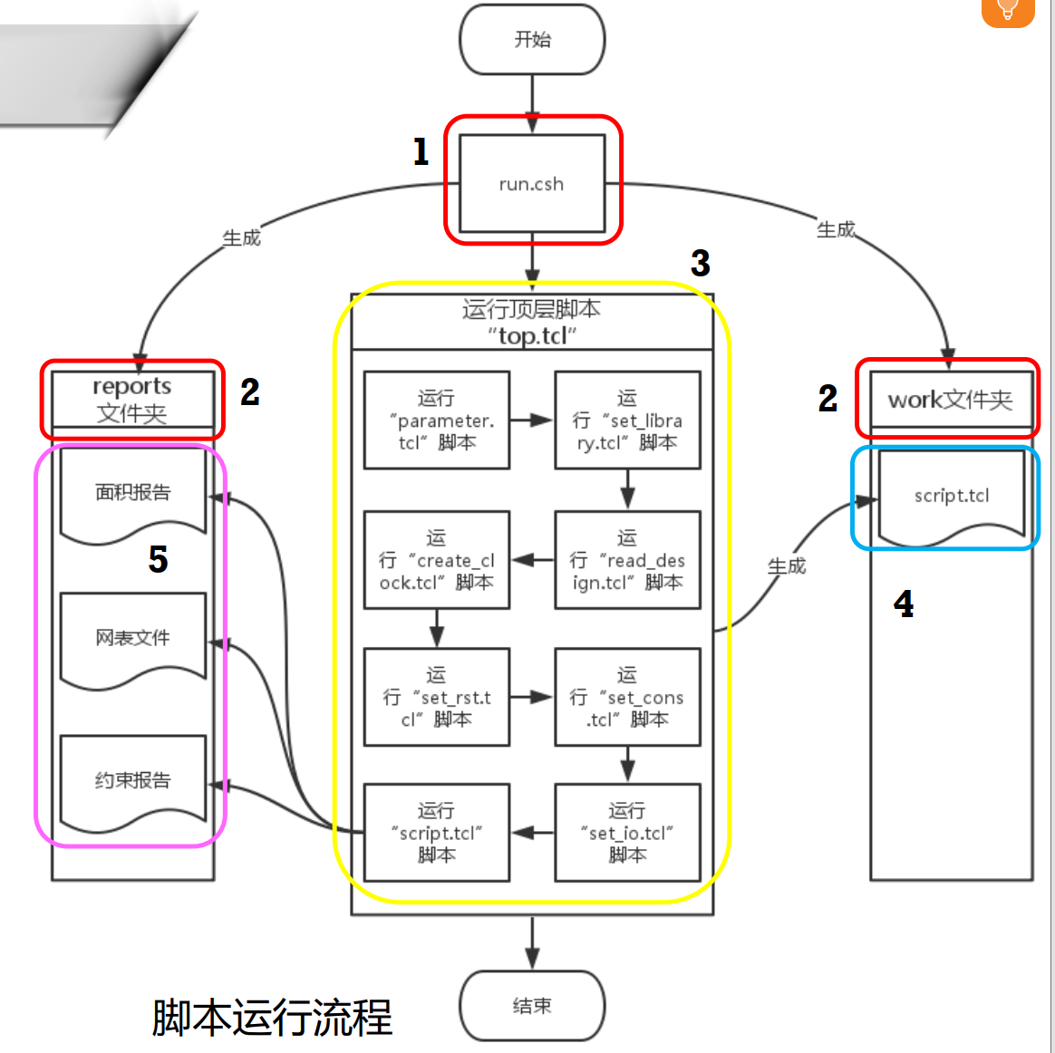
① 运行run.csh脚本,启动DC
1 | |
- top.tcl就是我们之后要写的自动化运行的TCL脚本,负责进行345所有的工作
② 建立reports与work两个文件夹。
- reports文件夹用于存放生成的报告,
- work文件夹用于存放该平台运行过程中生成的文档、脚本。
③ 启动顶层脚本top.tcl文件;
④ top.tcl按先后顺序启动各个子脚本,最终生成script.tcl;

- 运行script.tcl之前全部都是DC自动的,主要目的是生成约束脚本script.tcl,最终DC读取script.tcl通过它完成综合,并根据script.tcl生成报告
⑤ DC读取script.tcl中的约束,最终完成综合,并将所有报告写入reports文件夹中。
top.tcl脚本运行机制:生成DC所需要的约束文件.tcl,同意放进script.tcl来供DC去读取,所有流程自动
- set_library.tcl:生成设定库文件和search path的约束
- read_design.tcl:生成读入设计文件的约束
- 主要对所有verilog生成readverilog约束,写道script.tcl里面
- create_clock.tcl:生成时钟源相关的约束
- 这些约束也要生成到script.tcl里面
- set_rst.tcl:生成复位端口约束的约束
- set_io.tcl:生成输入输出端口的约束
- set_cons.tcl:生成保存门级网表、各种reprot文件的约束
注意:
- 以上所有约束都自动生成,无需人为干预;
- 库文件、代码、时钟、复位、输入输出等均根据代码自动进行匹配,并生成相应的约束;
- 最终所有的约束都被写入script.tcl中,供DC读取,完成最终的逻辑综合过程。
- 我们要做的就直接run就完事了,约束自动生成了,然后DC在跑
2)重要模块分析
(1)重要的脚本子模块——代码读入约束生成
- 工作流程:
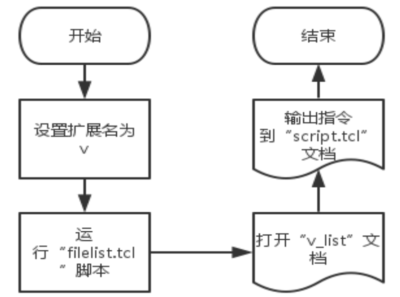
① 设计文件通常使用verilog语言,所以扩展名通常为v,所以先将变量extension设为v;
② 调用filelist.tcl脚本, filelist.tcl脚本会将所有扩展名为v的文件的文件路径输出到一个名为v_list的文档
③ 打开v_list文档,根据文件的内容将读入设计文件的指令输出到script.tcl脚本。
- 源码:
1 | |
(2)重要的脚本子模块——代码filelist生成模块filelist.tcl
功能:
本模块用filelist.tcl脚本实现,遍历目标文件下的所有文件,并将扩展名(.v)符合要求的文件完整路径输出到指定的文档,最终形成DC读取verilog代码的约束,写入script.tcl中。工作流程:
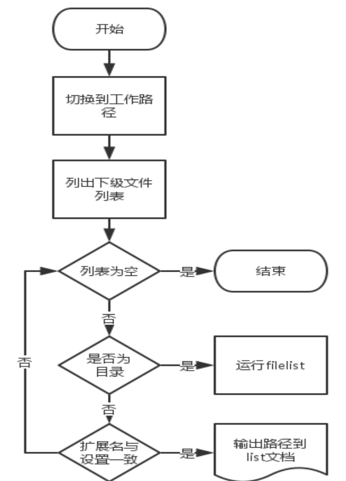
① 将工作路径切换到指定的工作路径
② 判断当前目录下的文件扩展名是否与设置的变量extension一致,如果一致,就将该文件路径输出到指定的文件
③ 如果有文件夹,则递归调用本程序,直至结束。
- 源码
1 | |
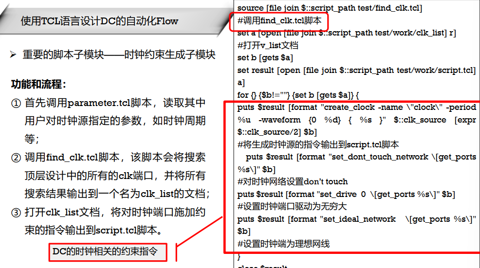
(3)重要的脚本子模块——时钟约束生成子模块
- 功能和流程:
① 首先调用parameter.tcl脚本, 读取其中用户对时钟源指定的参数, 如时钟周期等;
② 调用find_clk.tcl脚本, 该脚本会将搜索顶层设计中的所有的clk端口, 并将所有搜索结果输出到一个名为clk_list的文档;
③ 打开clk_list文档, 将对时钟端口施加约束的指令输出到script.tcl脚本
(4)重要的脚本子模块——匹配时钟端口子模块find_clk.tcl
功能:
搜索代码中的所有的时钟端口,将结果到work文件夹下的clk_list文档工作流程:
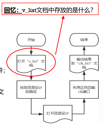
① 打开v_list文档,在其中找到顶层设计的路径,并打开改设计文件;
② 利用正则表达式匹配其中的clk端口;
③ 并将匹配到的时钟端口的端口名输出到work文件夹下的clk_list文档
(5)其余脚本工作机制
- 其余脚本工作机制类似。
- 最终,所有的约束都被写入了script.tcl中。script.tcl脚本完全由自动化电路综合平台生成并非人工编写;
- 在自动化电路综合平台运行后,由顶层脚本调用各子模块脚本生成该脚本。生成该脚本后,由顶层脚本调用该脚本,由此实现对设计的综合
3.4 参考书
- 《Using Tcl with Synopsys Tools》. Version B-2008.09, March 2011. Synopsys.
- 《集成电路静态时序分析与建模》. 刘峰, 机械工业出版社.出版时间: 2016-07-01
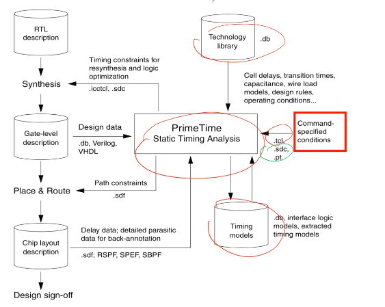
4 STA基本概念
- PrimeTime
- STA Conceptse
4.1 PrimerTime
PT是synopsys提出的全芯片过程中做STA的一个工具,在逻辑综合和PR的整个流程都很重要的存在
- PrimeTime is a full-chip, gate-level static timing analysis tool that is an essential part of
the design and analysis flow for today’s large chip designs. - PrimeTime exhaustively validates the timing performance of a design by checking all
possible paths for timing violations, without using logic simulation or test vectors. - PrimeTime fits ideally into the Synopsys physical synthesis flow because it uses many of the same libraries, databases, and commands as other Synopsys tools such as Design Compiler. It can also operate as a standalone static timing analyzer in other design flows
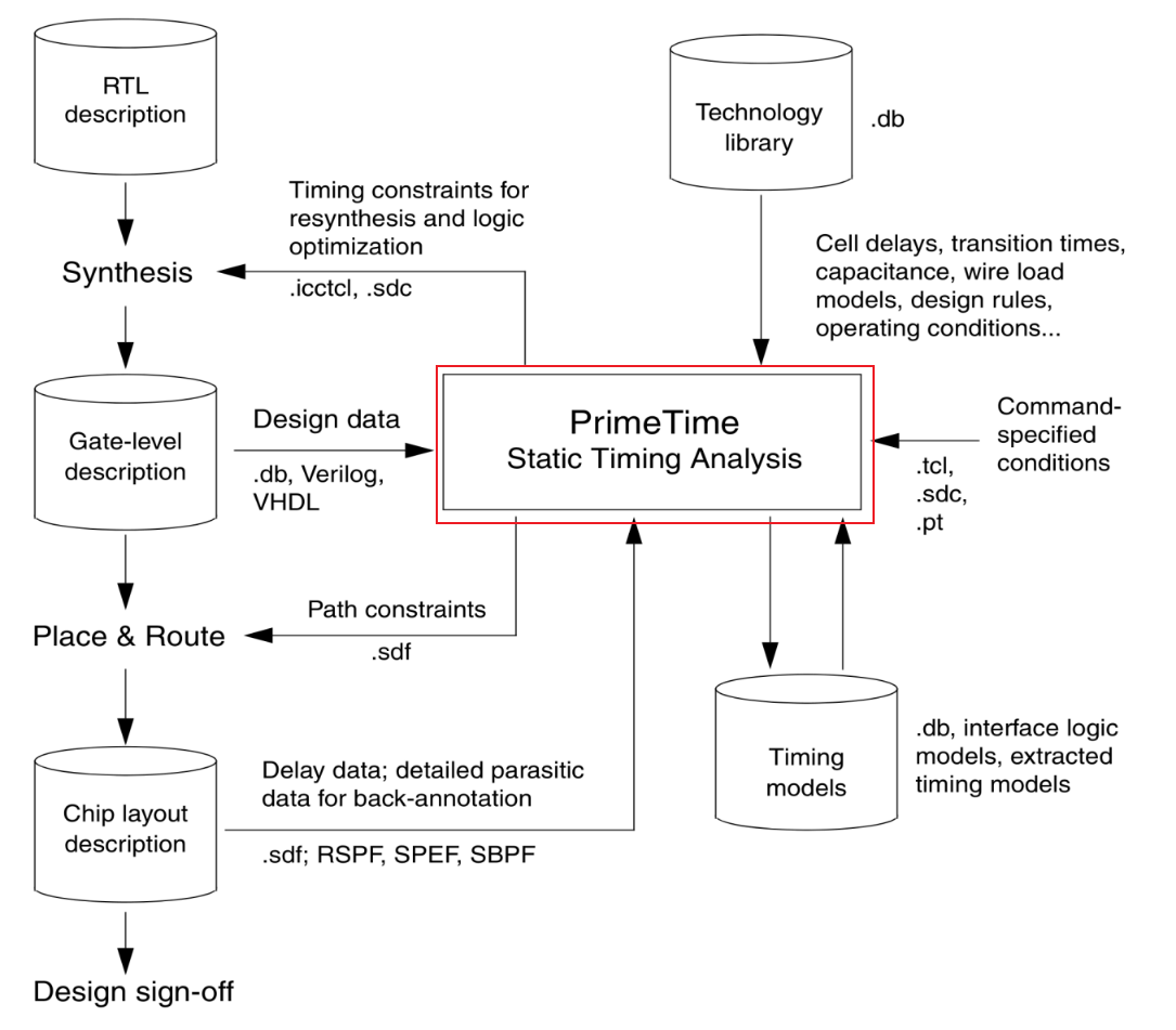
PT基于门级
PT在逻辑综合阶段和PR(Place & Route)阶段不一样,两种阶段的模型延迟精度不同,越往后时序分析模型越准确
静态时序中的库文件:
Technology library:库文件
Timing models:时序模型
2)两种运行模式
pt_shell
the graphical user interface (GUI). GUI中的命令行
4.2 STA Concepts
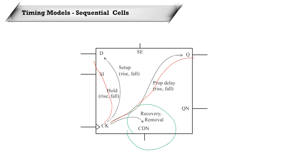
1)Timng Arc时序图
STA中的Timng Arc描述两个节点延迟信息的数据
Timing Arc分为:
连线延迟:单元输出端口和扇出网络负载之间的延迟信息
Cell delay单元延迟:单元输入端口和输出网络负载之间的延迟信息
- 完整的时序路径信息:连线延时+单元延时
2)Cell delay
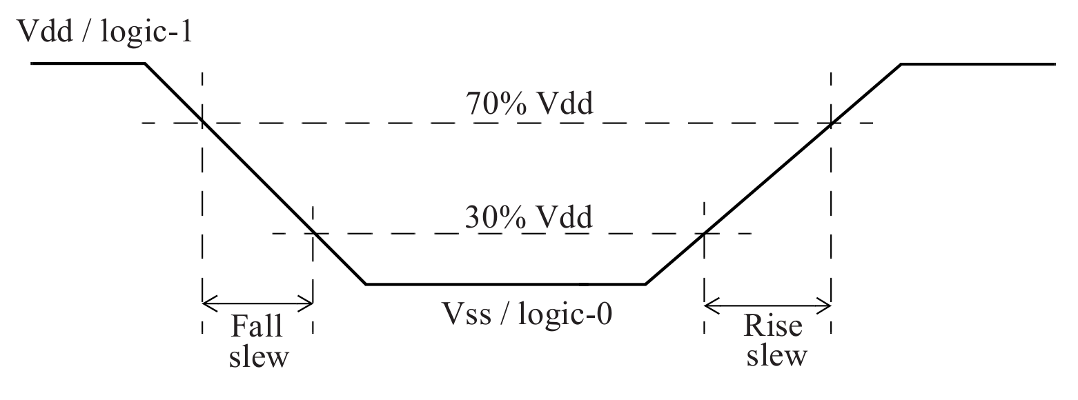
(1)Transition delay:信号翻转延迟
- 分为两种:0—>1或者1—>0
(2)Logic gate delay:Cell由输入端口到输出端口的延迟
3)Setup time and hold time
Setup time:
- Setup time:A setup constraint specifies how much time is necessary for data to be available at the input of a sequential device before the clock edge that captures the data in the device
- This constraint enforces a maximum delay on the data path relative to the clock path. (通过建立时间限制整个电路的最大延迟值)
- 两种Path
Hold time:
A hold constraint specifies how much time is necessary for data to be stable at the input of a sequential device after the clock edge that captures the data in the device.
This constraint enforces a minimum delay on the data path relative to the clock path.(最小延迟)

4)Timg path时序路径
- STA把电路划分为不同的时序路径,然后分析每一条路径上的st和ht是否符合要求的约束
- 每一条Time path包括起点和终点,一定要分清pin和port

Time path startpoint有两种:
- a clock pin of a sequential element, or possibly an input port of the design (because the input data can be launched from some external source).
- startpoint in below design:D_clk_pin , A_input_port
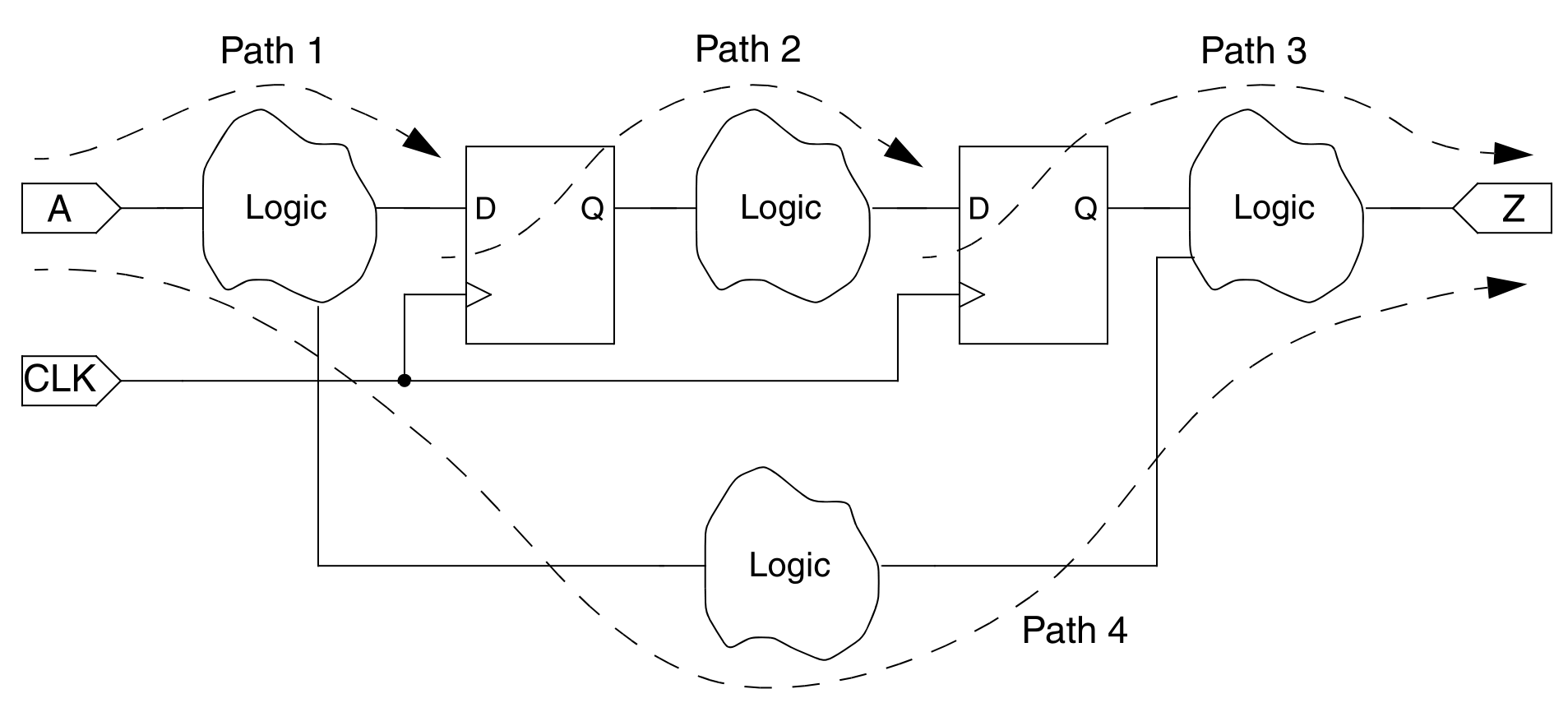
Time path endpoint有两种:
- a data input pin of a sequential element, or possibly an output port of the design (because the output data can be captured by some external sink).
- endpoint in below design:D_clk_pin , Z_output_port

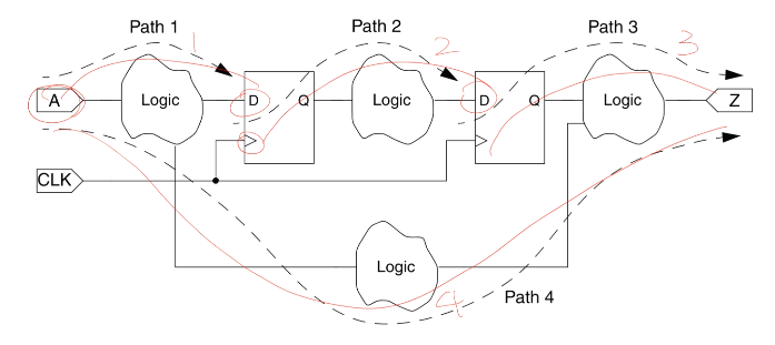
上述Path1~4的分析
- 这种定义(time path , start ,begin)覆盖了每一条门级路径
- 任何路径都会被划分为4种(两种起点*两种重点=4种path),一定要分清pin和port:
- clk pin -> D
- clk pin -> output port
- input -> D
- input -> output port
- diff between pin & port:
- pin for cell
- port for core
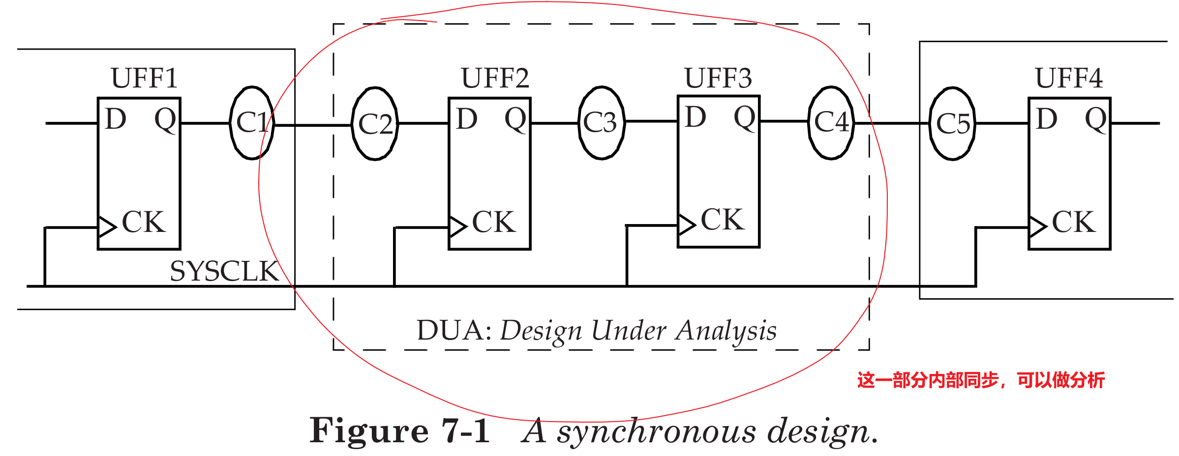
5)Clock Domains时钟域
如今大部分芯片都是全局异步、局部同步,如下所示:

DC/PT处理同步电路,对异步电路无能为力的。因此我们在做整体分析时:
- 首先根据时钟域区分哪些是同步电路,哪些是异步电路
- 对局部的同步电路使用PT/DC综合和分析
- 对跨时钟域电路进行一些时钟约束(定义一些时序的路径),让PT知道这部分我们无法做STA
6)Operating Condition操作条件
Operating Condition操作条件:
Static timing analysis is typically performed at a specific operating condition.
STA时需要指定条件,才能对该特定条件cell或线进行检查,是否满足setup、hold
An operating condition is defined as a combination of PVT: Process(工艺制成), Voltage(电压) and Temperature (温度)
operation condition条件指的是PVT
Cell delays and interconnect delays are computed based upon the specified operating
condition.cell和互连线的delay必须是基于特定的PVT,才能进行精准分析
There are three kinds of manufacturing process models that are provided by the
semiconductor foundry for digital designs: slow process models, typical process models,and fast process models.PVT分为三种:slow,typical,fast
The slow and fast process models represent the extreme corners of the manufacturing process of a foundry.
slow,fast通常是极限条件进行测试
For robust design, the design is validated at the extreme corners of the manufacturing process as well as environment extremes for temperature and power supply.
PVT与delay的关系:
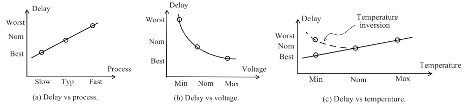
- 高温+低电压:确保延迟最差/慢,ss->max->check setup
- 低温+高电压:确保延迟最小,ff->min->check hold
- 典型值没有ff和ss有代表性
PVT的数值表现在库中:
The choice of what operating condition to use for STA is also governed by the operating conditions under which cell libraries are available. Three standard operating conditions are:
一下是我们假设的等级的通常要求
- WCS (Worst-Case Slow):
- Process is slow, temperature is highest (say 125C) and voltage is lowest (say nominal 1.2V minus 10%)
- BCF (Best-Case Fast):
- Process is fast, temperature is lowest (say -40C) and voltage is highest (say nominal 1.2V plus 10%).
- TYP (Typical):
- Process is typical, temperature is nominal (say 25C) and voltage is nominal (say 1.2V).
SynopsysTCL指定操作条件:
1 | |
4.3 参考书
- Static Timing Analysis for Nanometer Designs: A Practical Approach. J.Bhasker, Rakesh Chadha. Springer Science Business Media, LLC 2009.Chaper 2.
- 集成电路静态时序分析与建模. 刘峰, 机械工业出版社.出版时间: 2016-07-01.第二章.
- PrimeTime ® Fundamentals User Guide. Synopsys. Version F-2011.12,December 2011
5 标准单元库
- Overview of Synopsys Timing lib(时序库)
- Non-Linear Delay Model
- Threshold Specifications and Slew Derating
- Timing Models
- Wire Delay Models
5.1 Timing lib时序库
库的基本概念

两种格式不同内容相同的库:
.db格式的库打不开
.lib格式的库可以打开看,如下图:
一个标准单元的工艺库(cell lib):
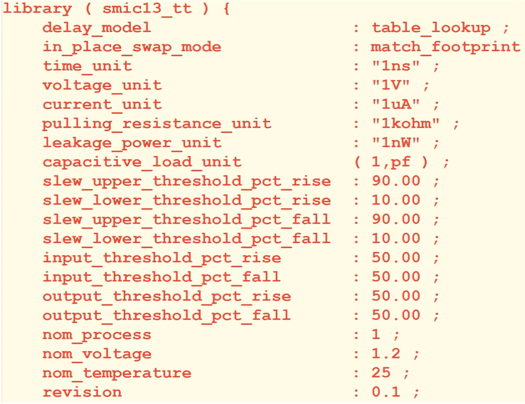
- delay_model:lookuptable
- 由查找表来实现延迟模型
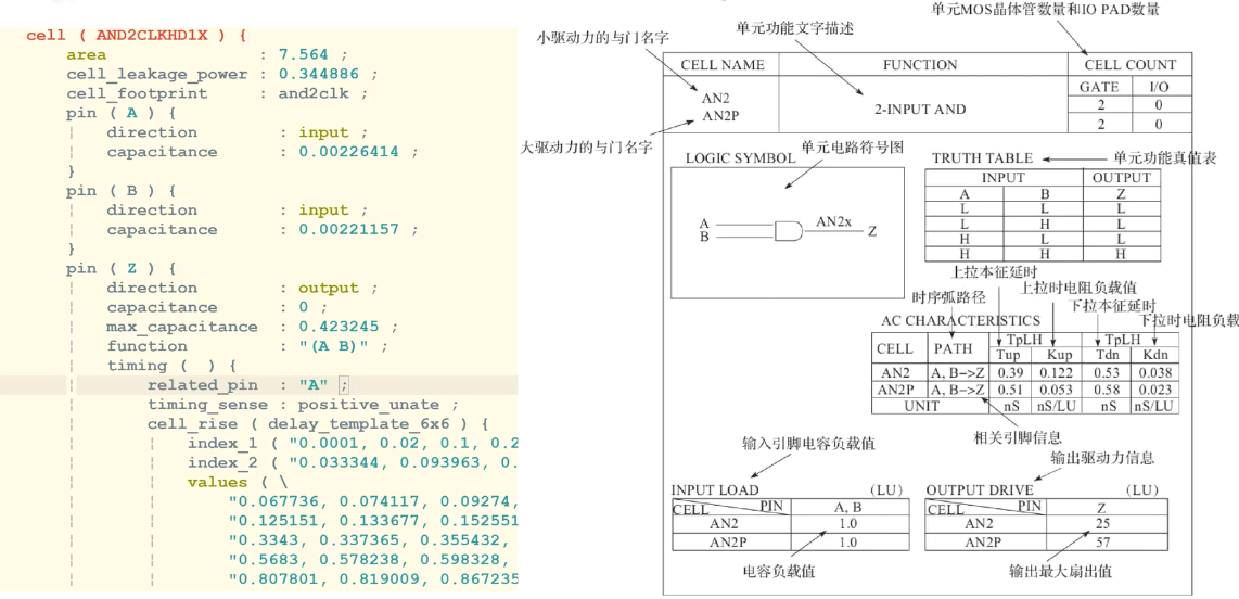
- Value对应的查找表
5.2 Non-Linear Delay Model非线性的延迟模型
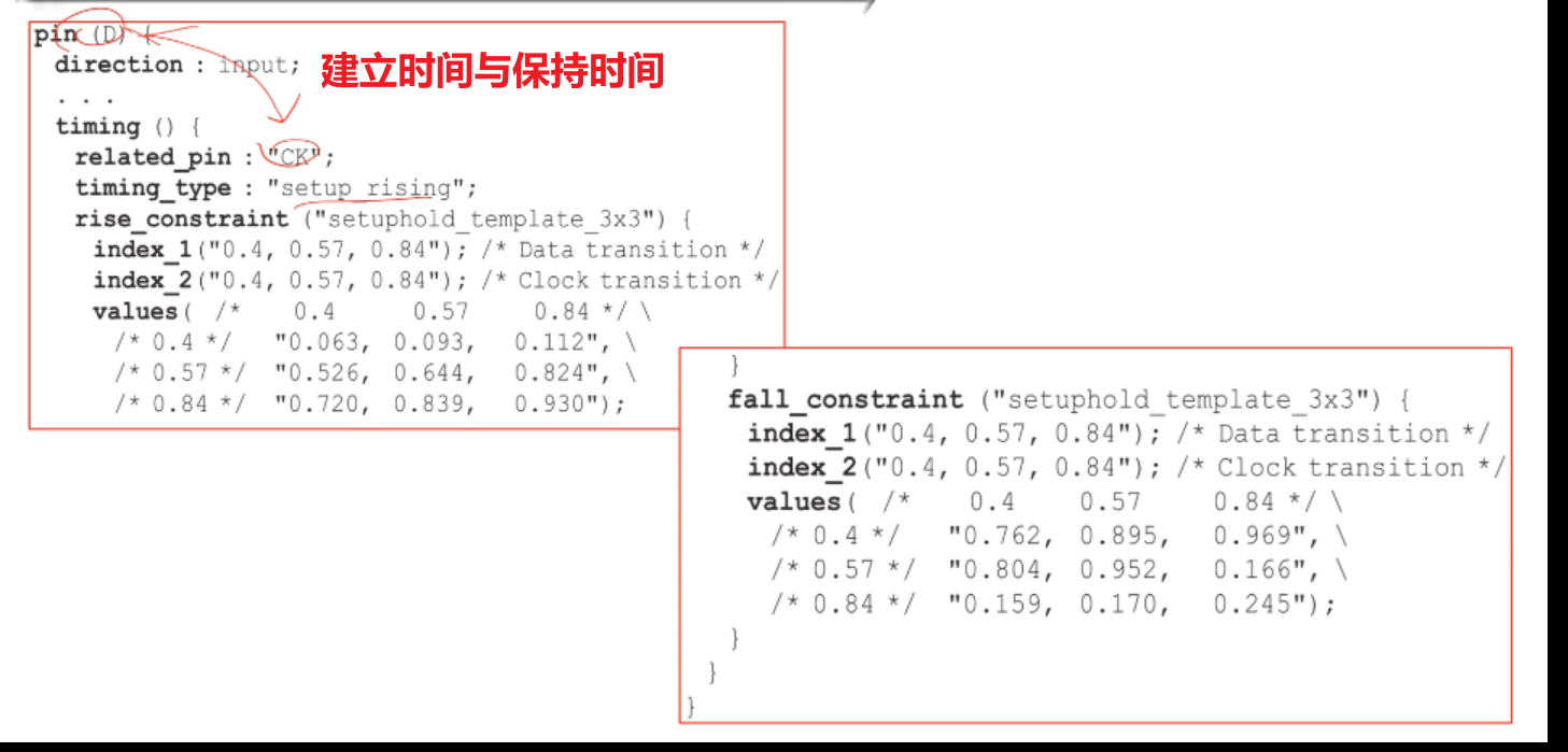
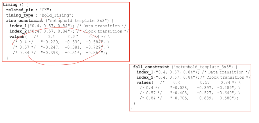
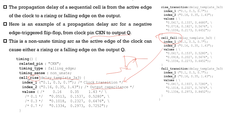
1)反相器实例分析:
Let us first consider timing arcs for a simple inverter logic. Since it is an inverter, a rising (falling) transition at the input causes a falling (rising) transition at the output.
The two kinds of delay characterized for the cell are(两种延迟特征/延迟值):
- Tr:Output rise delay(输入下降输出上升延迟)
- Tf:Output fall delay(输入上升输出下降延迟)
Notice that the delays are measured based upon the threshold points defined in a cell ibrary, which is typically 50% Vdd.
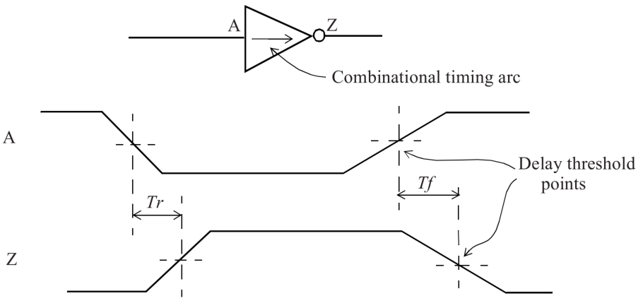
STA中的时序模型Time Arc取决于两个因素:
- 输出的负载(输出引脚的电容负载)
- 输入的transition time转化时间
- 大多数情况下延迟会随着输入transition增加而增加
确定输入的转化时间和输出电容后,标准单元可以跟时序的模型来计算或查询延迟信息,通常来说标准单元的延迟模型有两种:
- 线性的
非线性的
2)一种通用的线性延迟模型公式:
1 | |
- 通过上述模型可以计算当前的延迟信息有多少
- 随着半导体工艺发展,这种线性模型越来越不准确率,实际应用较少
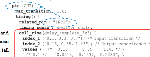
3)NLDM非线性延迟模型
NLDM非线性延迟模型计算方法:
- 在cell lib标准库文件中通过一个二维的查找表构成延迟模型
Here is an example of such a table for a typical inverter cell:
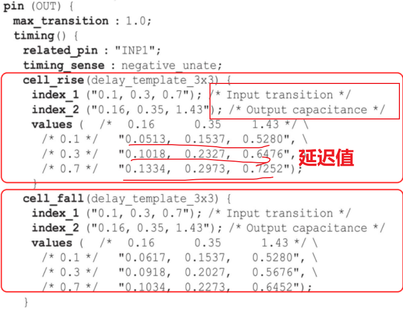
模型方向:
传输时间和电容对应不上时:
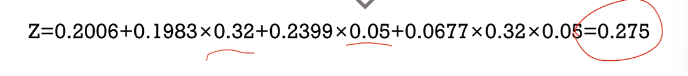
- 通过插值计算/高斯消元法
- 实例分析
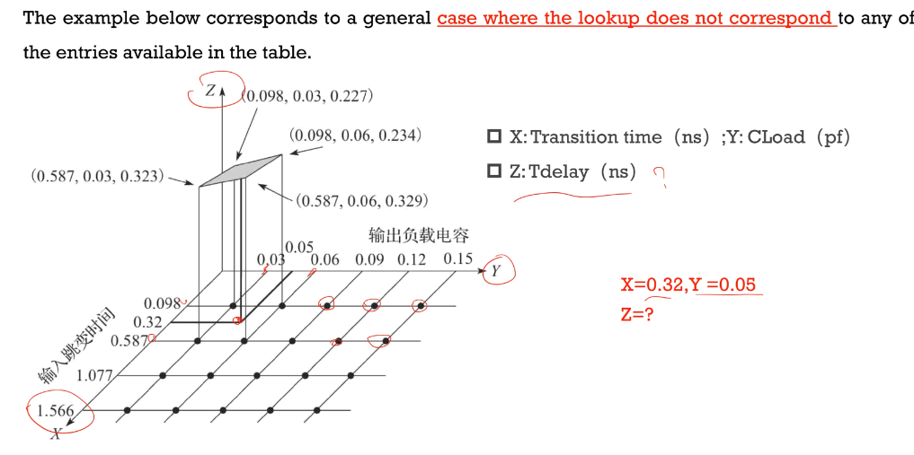
高斯消元法计算过程:
- 思想:一个点用周围四个点计算
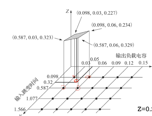
- 高斯消元法固定公式:
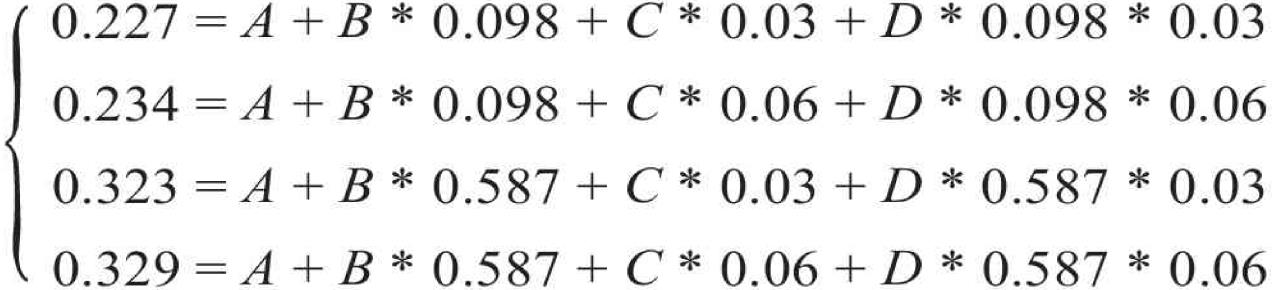
- 步骤1:周围四个点带入公式求解ABCD
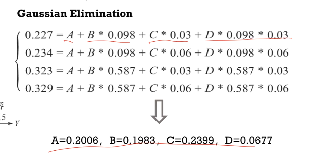
- 步骤2:计算Z
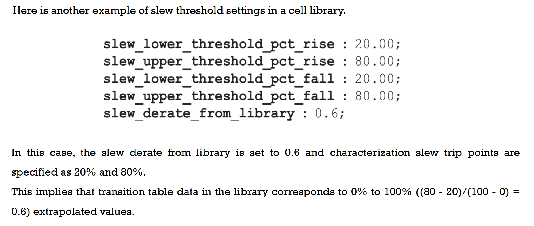
5.3 Threshold Specifications and Slew Derating(使用缩放确定查找表的表项)
我们的库中一般是10%~90%的电压测量的延迟
The slew 1 values are based upon the measurement thresholds specified in the library. Most of the previous generation libraries (0.25?m or older) used 10% and 90% as measurement thresholds for slew or transition time.
实际工艺中更多的是30%~70%,而库里面早期是10%~90%
The slew thresholds are chosen to correspond to the linear portion of the waveform. As technology becomes finer, the portion where the actual waveform is most linear is typically between 30% and 70% points.
Thus, most of the newer generation timing libraries specify slew measurement points as 30% and 70% of Vdd
Slew:从10~90缩小到30~79
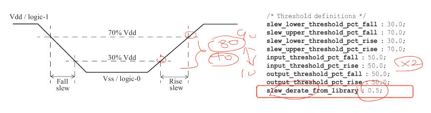
However, because the transition times were previously measured between 10% and 90%, the transition times measured between 30% and 70% are usually doubled for populating the library. This is specified by the slew derate factor which is typically specified as 0.5.
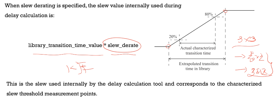
The slew thresholds of 30% and 70% with slew derate as 0.5 results in equivalent measurement points of 10% and 90%. An example settings of threshold is illustrated below.
对应实际库:
During characterization, the transition is measured at 30-70 and the transition data in the library corresponds to extrapolation of measured values to 10% to 90% ((70 - 30)/(90 - 10) = 0.5)

The above settings specify that the transition times in the library tables have to be multiplied by 0.5 to obtain the transition times which correspond to the slew threshold (30-70) settings.
This means that the values in the transition tables (as well as corresponding index values) are effectively 10-90 values.
也可以不指定
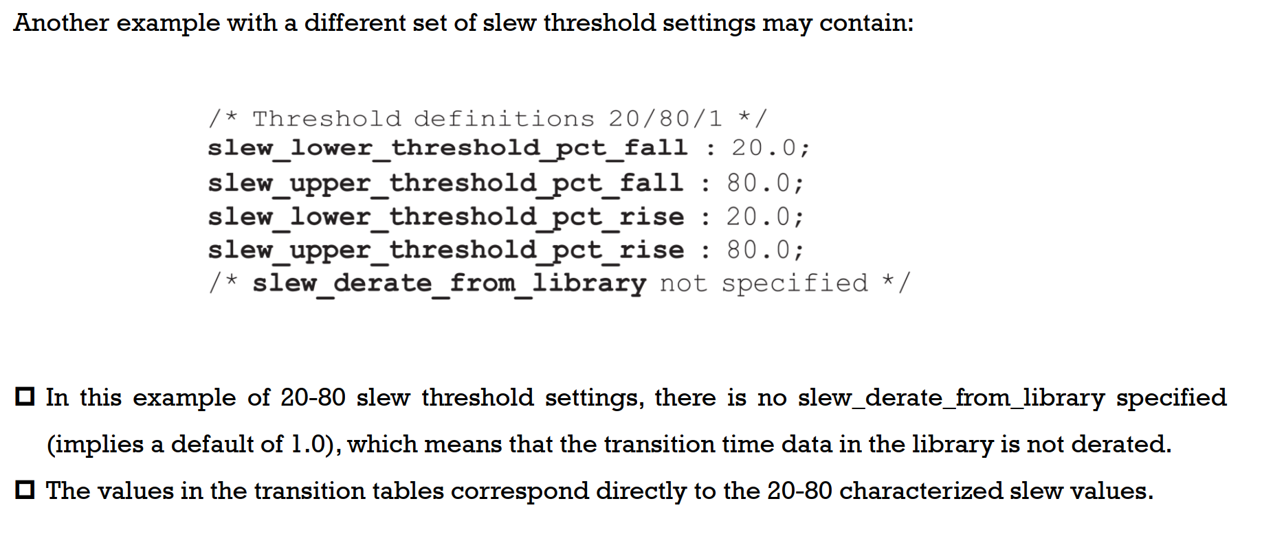
也可指定其他值
应用场景:
- 自己建库
- K库
- 设计低功耗芯片时,需要从新建一套,需要缩小电压值,在已有的库上做扩展:
- 此时表项、延迟都不一样了,需要在已有库上做抽取,从而形成新的查找表
- 设计低功耗芯片时,需要从新建一套,需要缩小电压值,在已有的库上做扩展:
5.4 Timing Model时序模型
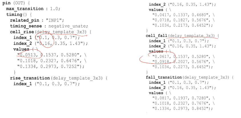
1)两输入与门示例
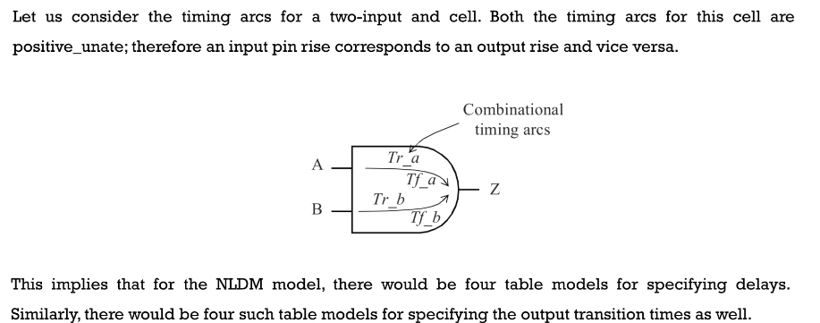
库内信息:
2)时序的Cell示例
库内信息:
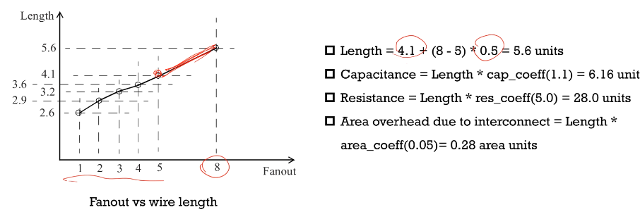
5.5 线延迟模型
用分布式RC树来抽象互连线,主要两种模型:(参考数字集成电路书)
- T模型
- Pi模型

线模型示例库内信息
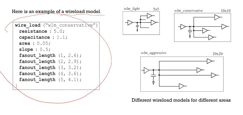
- area面积
- slope斜率
- _length线长
超出线长时的计算方法:使用斜率计算
6 STA环境配置(重要)
- What is the STA Environment?
- Specifying Clocks
- Generated Clocks
- Constraining Input Paths and Output Path
- Design Rule Checks
- Virtual Clocks
- Refining the Timing Analysis
本次课主要求如何撰写、指导、分析整个sta中的sdc约束
PrimeTime:
使用约束可以在synthesis、PR、sign-off进行静态时序分析
6.1 STA Env
- 我来给STA指定一个约束,
- 约束严谨、精确才能指导STA对整个电路做一个全面且正确的检查
- 才能确定setup、hold是真正满足需求,否则给一个错误的约束可能STA错误
- ENV包括:时钟、IO、指定时序路径的特殊约束
STA针对同步电路,对异步电路无能为力:
6.2 Specifying Clocks时钟约束(重要)
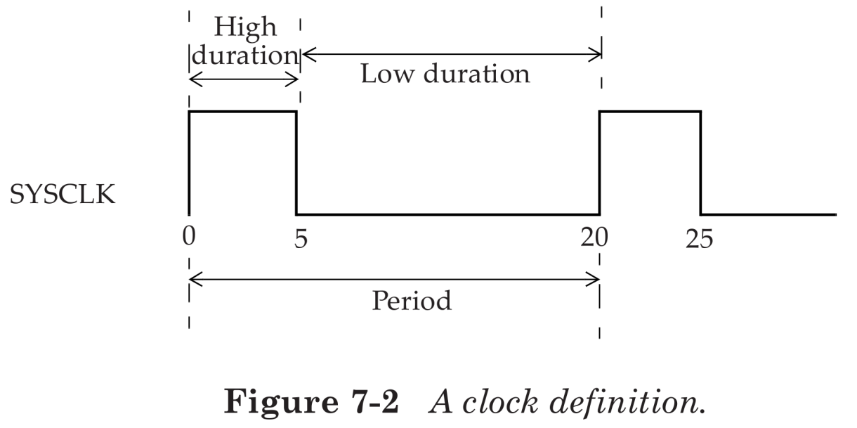
1)Specifying Clocks | 时钟约束的形状
To define a clock, we need to provide the following information:
- Clock source时钟源: it can be a port of the design, or be a pin of a cell inside the design (typically that is part of a clock generation logic).
- Period周期: the time period of the clock.
- Duty cycle占空比: the high duration (positive phase) and the low duration (negative phase).
- Edge times边缘翻转时间: the times for the rising edge and the falling edge.
clock的sdc约束条件代码示例:
- 所有sdc的约束都是按照TCL/Synopsys TCL的语法来写的
1 | |
其他的定义示例:
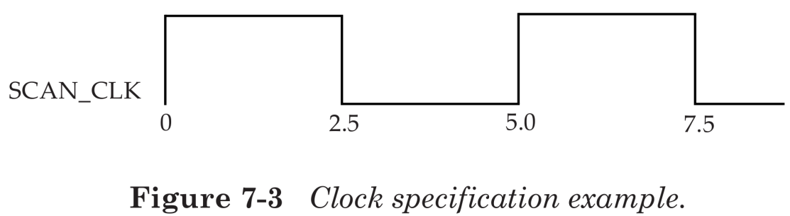
1 | |
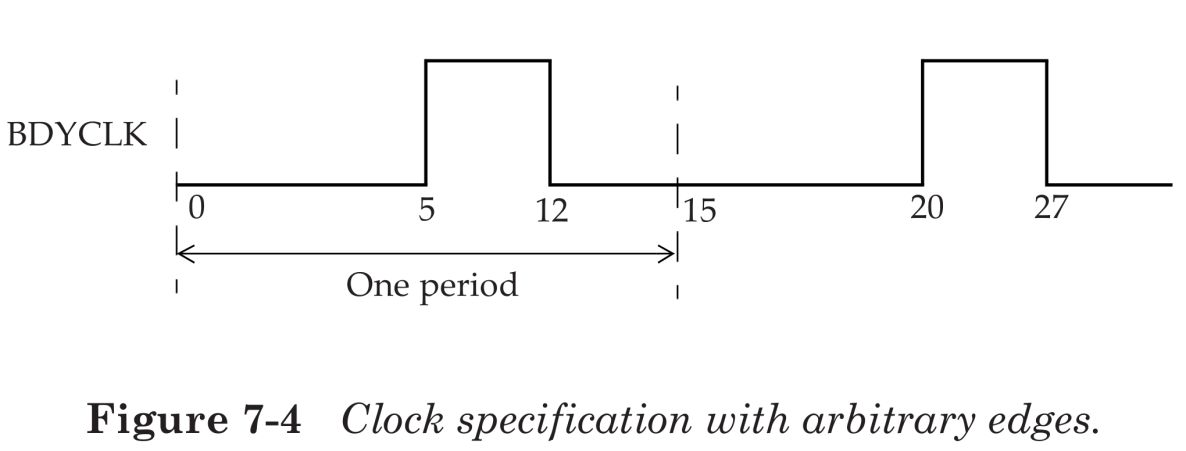
1 | |
2)Specifying Clocks-Clock Uncertainty
前面我们描述了时钟的形状,但时钟存在误差(时钟偏斜、clock jitter等等),我们通过set_clock_uncertainty来对时钟误差进行估计或更严格的指定
- 更严格可以认为是有效时钟周期的减小
- 通过比较悲观的设计使得设计变得稳健
- 也可对虚拟时钟进行指定
uncertainty定义示例1:
1 | |
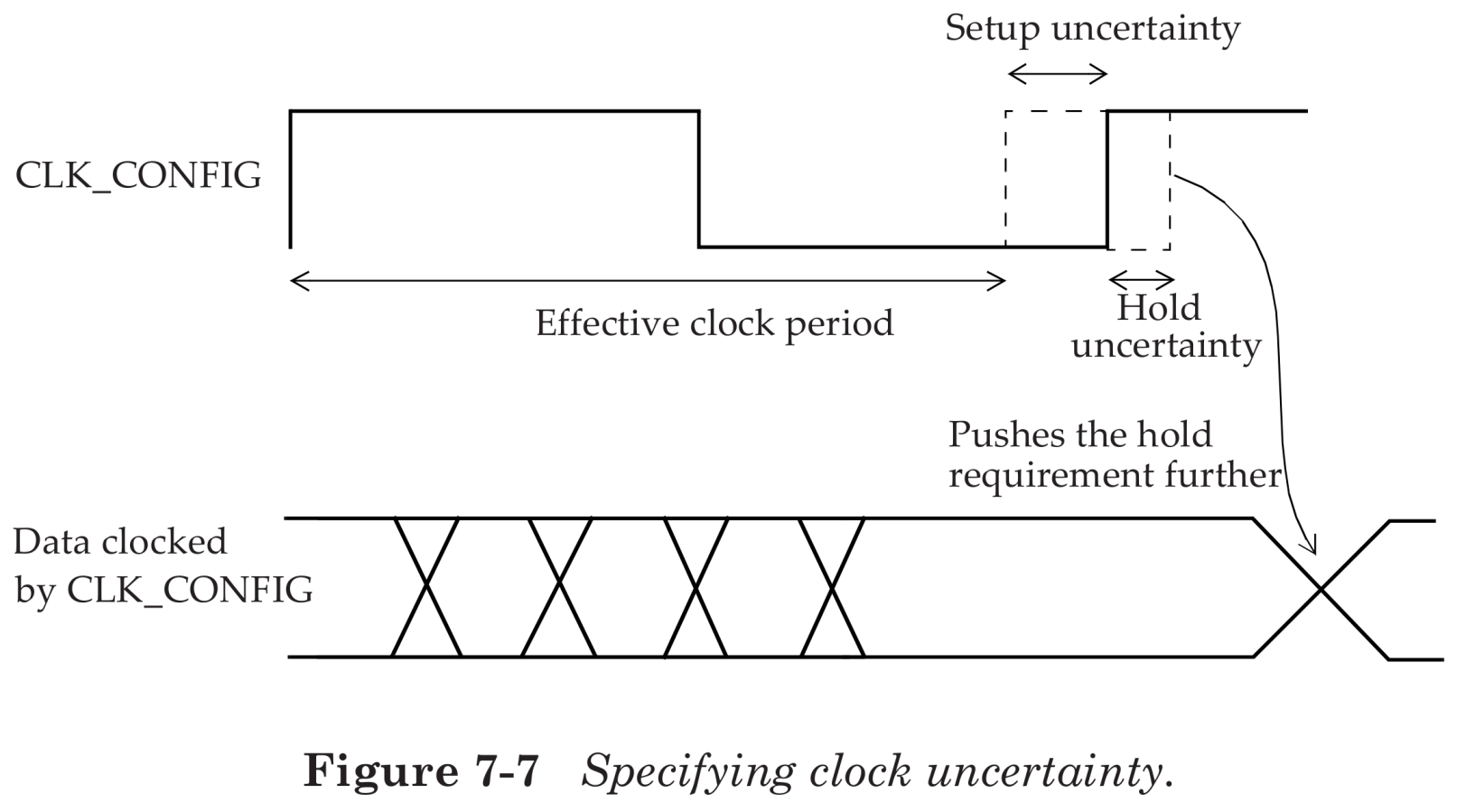
uncertainty定义示例2——针对两个时钟的指定:
1 | |

进一步解释uncertainty作用方法——实现时钟偏差
- Clock Skew时钟偏差
- Clock Jitter时钟抖动
- Clock Delay时钟延迟
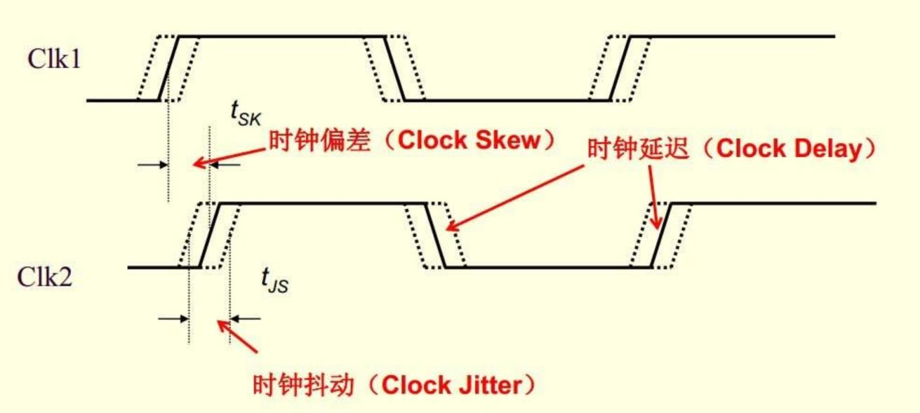
- 我们做时钟树的时候要求尽可能的减小偏差,而uncertainty产生时钟偏差从而构造一种更严格的环境
3)时钟延迟
两种latency,都需要计算:
- Network latency is the delay from the clock definition point (create_clock) to the clock pin of a flip-flop
- 定义的时钟节点到触发器
- Source latency, also called insertion delay, is the delay from the clock source to the clock definition point
- 时钟源到定义节点
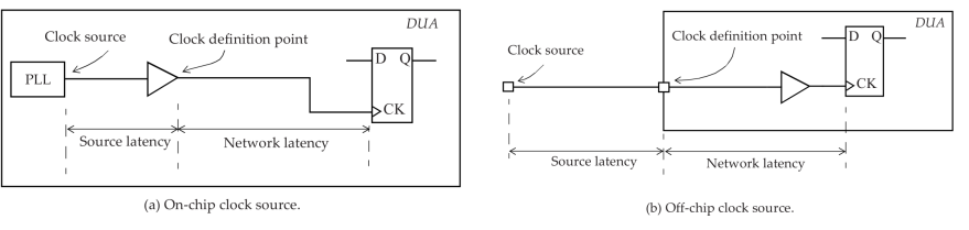
如何通过TCL脚本指定latency:
1 | |
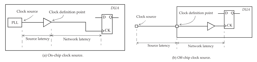
latency 总结:
- One important distinction to observe between source and network latency is that once a clock tree is built for a design, the network latency can be ignored (assuming set_propagated_clock command is specified).
- latency的区别:
- 如果时钟树已经建立好,你的得到的latency则是非常精确的
- 如果在PR之前,在DC的时候,你的时钟树综合之前,latency是个估计的
- latency的区别:
- However, the source latency remains even after the clock tree is built.
- The network latency is an estimate of the delay of the clock tree prior to clock tree synthesis.
- After clock tree synthesis, the total clock latency from clock source to a clock pin of a flip-flop is
the source latency plus the actual delay of the clock tree from the clock definition point to the
flip-flop.
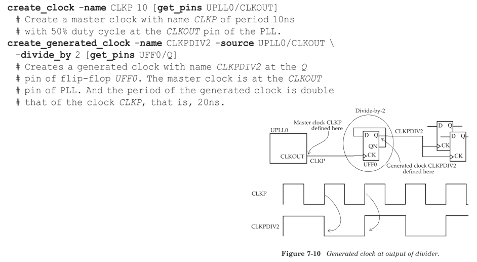
6.3 Generated Clock 生成时钟
Generated Clock & Master Clock:
- A generated clock is a clock derived from a master clock. A master clock is a clock defined using the create_clock specification.
- When a new clock is generated in a design that is based on a master clock, the new clock can be defined as a generated clock.
Generated Clock定义的作用:This definition is needed as STA does not know that the clock period has changed at the output of the divide-by logic, and more importantly what the new clock period is
Generated Clock如何定义:
create_clockcreate_generated_clock -source(required) -divide_by <num>(num option,下图中指的是2分频)
可以把generated clock定义为master clock,因此不要定义为master时钟,这样静态时序会乱,特殊情况下可以定义
generated clock定义成新的时钟带来的问题:
- (问题一)两个clock之间失去了联系,作为时序分析时STA认为互为异步时钟而不是同步时钟
Can a new clock, that is, a master clock, be defined at the output of the flipflop instead of a generated clock? The answer is yes, that it is indeed possible. However, there are some disadvantages. Defining a master clock instead of a generated clock creates a new clock domain.
Defining the new clock as a generated clock does not create a new clock domain, and the generated clock is considered to be in phase with its master clock. The generated clock does not require additional constraints to be developed. Thus, one must attempt to define a new internally generated clock as a generated clock instead of deciding to declare it as another master clock.
- (问题二)成为新的时钟的源点,与原来的mclk没有寄生关系了:
Another important difference between a master clock and a generated clock is the notion of clock origin. In a master clock, the origin of the clock is at the point of definition of the master clock. In a generated clock, the clock origin is that of the master clock and not that of the generated clock.4
This implies that in a clock path report, the start point of a clock path is always the master clock definition point. This is a big advantage of a generated clock over defining a new master clock as the source latency is not automatically included for the case of a new master clock.
- mclk&gclk
Clock latencies can be specified for generated clocks as well.
A source latency specified on a generated clock specifies the latency from the definition of the master clock to the definition of the generated clock.
The total clock latency to a clock pin of a flop-flop being driven by a generated clock is thus the sum of the source latency of the master clock, the source latency of the generated clock and the network latency of the generated clock

- (特例)什么时候可以定义为master
- 下图是两个clk的与生成的新时钟
- 同时推荐写gclk约束之前画一下时钟树,清楚时钟区域
If the input to the and cell are both clocks, then it is safe to define a new main clock at the output of the and cell, since it is highly unlikely that the output of the cell has any phase relationship with either of the input clocks
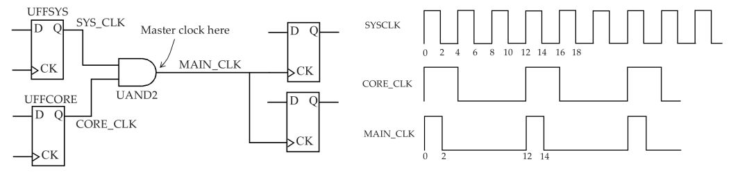
- 上述两与门clk的约束写法:
If the input to the and cell are both clocks, then it is safe to define a new main clock at the output of the and cell, since it is highly unlikely that the output of the cell has any phase relationship with either of the input clocks.

Generated Clock使用情况很多:
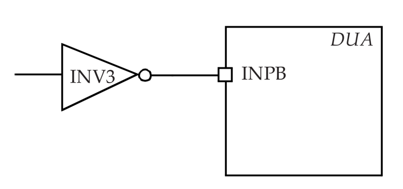
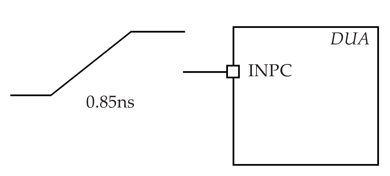
6.4 Constraining Input Paths & Output Path
1)示意图
我们讨论时序路径主要是分析从reg到reg
时序路径:INP1->UFF1.D
- 这种路径不存在时钟,需要对INP1增加input delay
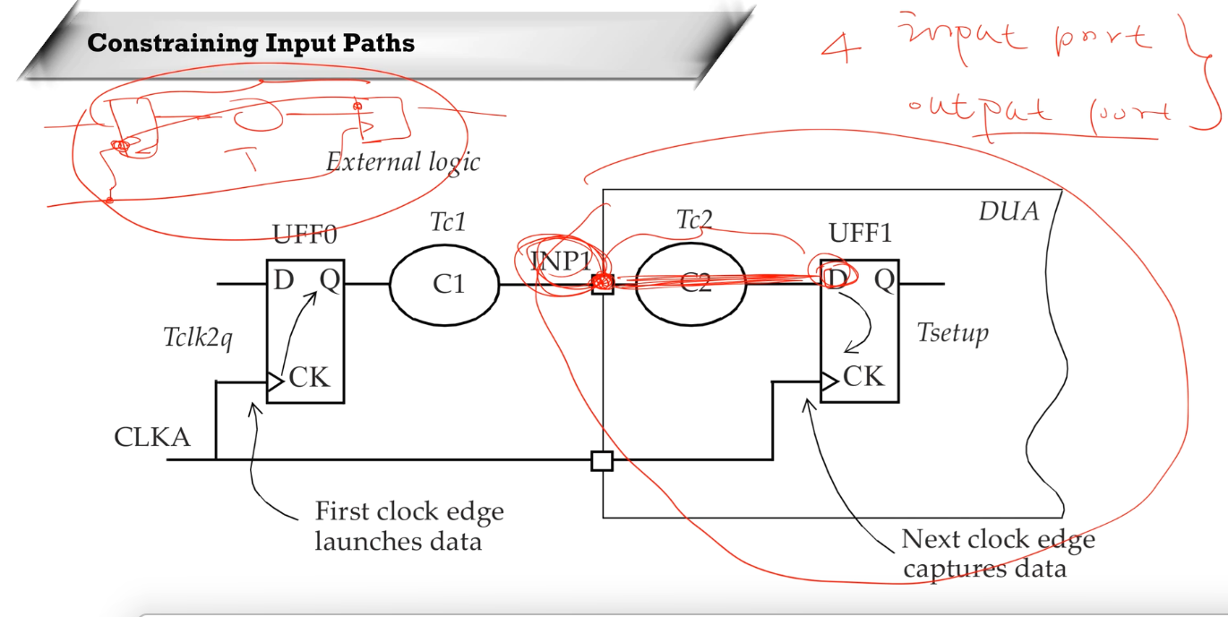
约束指令示例:set_input_delay
- set_input_delay:
- CLKA(时钟域/时钟引脚)
- 约束值(一个区间/比例)
1 | |
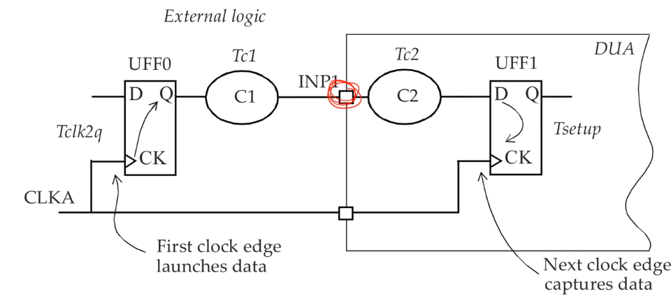
input——setup,hold time,max,min分别设置
- 注意max和min
1 | |
output约束类似
1 | |
output——setup,hold time,max,min分别设置
1 | |
四种时钟约束路径总结
至此我们学过了全部四种的时钟路径
Timing Path Groups路径组
电路内部时序复杂,有很多时钟,如何判断始于哪个时钟域/时钟组:
- 查看endpoint终点,终点属于哪个时钟,就属于哪一时钟的path group
Timing paths are sorted into path groups by the clock associated with the endpoint of the path. Thus, each clock has a set of paths associated with it.
There is also a default path group that includes all non-clocked (asynchronous) paths.
额外属性(在指定端口时的额外属性)
While create_clock, set_input_delay and set_output_delay are enough to constrain all paths in a design for performing timing analysis, these are not enough to obtain accurate timing for the IO pins of the block.
The following attributes are also required to accurately model the environment of a design.
对input来讲:
- set_driver
- 设置驱动强度,值越小越大,0为无限大(理想状态),但还是需要都设置一下不要都设为理想
- set_driving_cell
- set_input_transition
对output
For outputs, one needs to specify the capacitive load seen by the output pin. This is specified by using the following specification:
- set_load
input
具体设置情况
The set_drive explicitly specifies a value for the drive resistance at the input pin of the DUA. The smaller the drive value, the higher the drive strength.
A resistance value of 0 implies an infinite drive strength.
1 | |
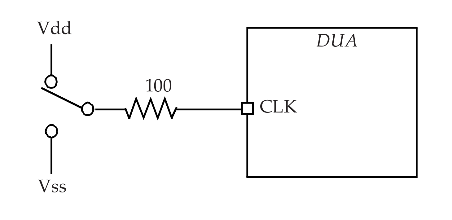
- 根据驱动能力,如何计算第一个门的延迟能力
The drive of an input port is used to calculate the transition time at the first cell. The drive value specified is also used to compute the delay from the input port to the first cell in the presence of any
RC interconnect.
1 | |
从库里面设置driver(简单):
关于port补充内容,多翻一下synopsys手册以及刘老师的静态时序分析、建模:
get_ports <PIN>all_inputs
1 | |
1 | |
总结
- 缺省状态下的驱动能力为理想状态(0)与实际不符
In summary, a slew value at an input is needed to determine the delay of the first cell in the input
path.
In the absence of this specification, an ideal transition value of 0 is assumed, which may not be
realistic.
output
对于output我们关心capacitive load(电容负载),默认为0,我们需要把load改为不为理想值
The set_load specification places a capacitive load on output ports to model the external load being
driven by the output port.By default, the capacitive load on ports is 0. The load can be specified as an explicit capacitance value
or as an input pin capacitance of a cell
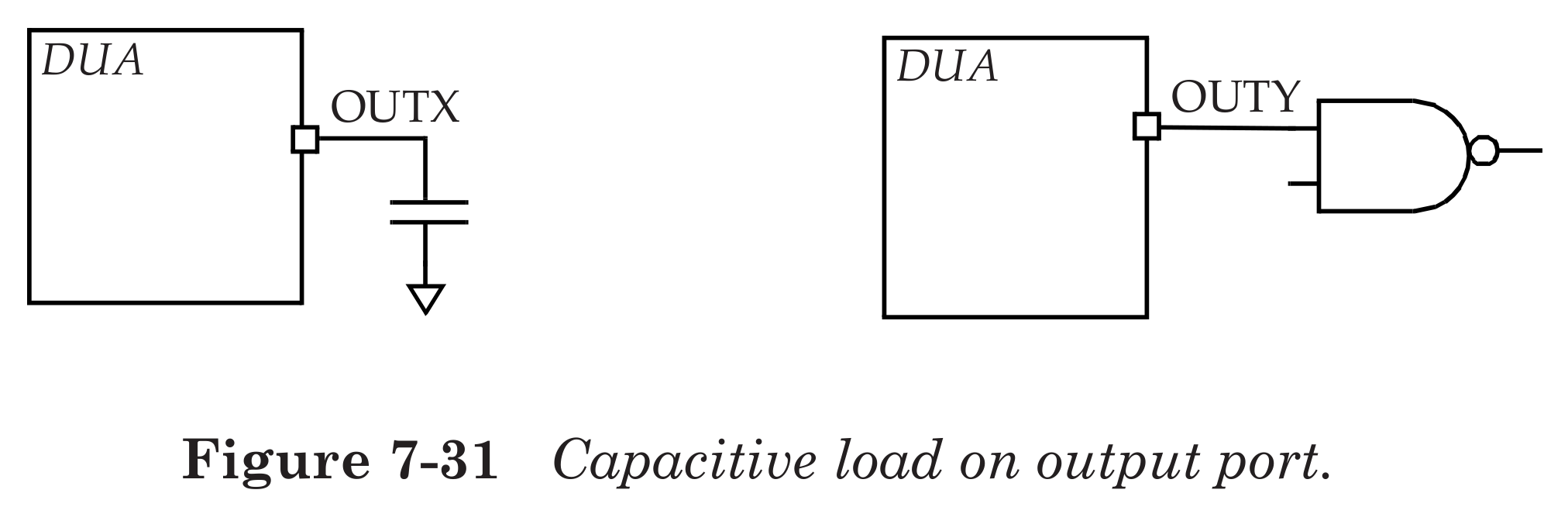
具体设置情况
- port
- all_output
- 过滤
1 | |
It is important to specify the load on outputs since this value impacts the delay of the cell driving the output. In the absence of such a specification, a load of 0 is assumed which may not be realistic
1 | |
6.5 DRC(Design Rule Checks)
STA中用到最多的:max transition and max capacitance
DRC主要检查所有的port和pin是否满足the specified limits for transition time 1 and capacitance
通常来讲TCL指定方式为:
- set_max_transition
- set_max_capacitance
使用不是特别多的指令(在时序中使用不是特别直接),通常更关心上面两个
- set_max_fanout (specifies a fanout limit on all pins in design)
- set_max_area (for a design);
使用示例
1 | |
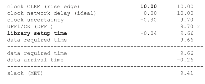
6.6 Virtual Clock 虚拟时钟
虚拟时钟与design中的pin无关,主要在STA中做参考,来指定input port或output port的相关时钟
由于虚拟时钟在电路中没有引脚,因此不需要get_ports
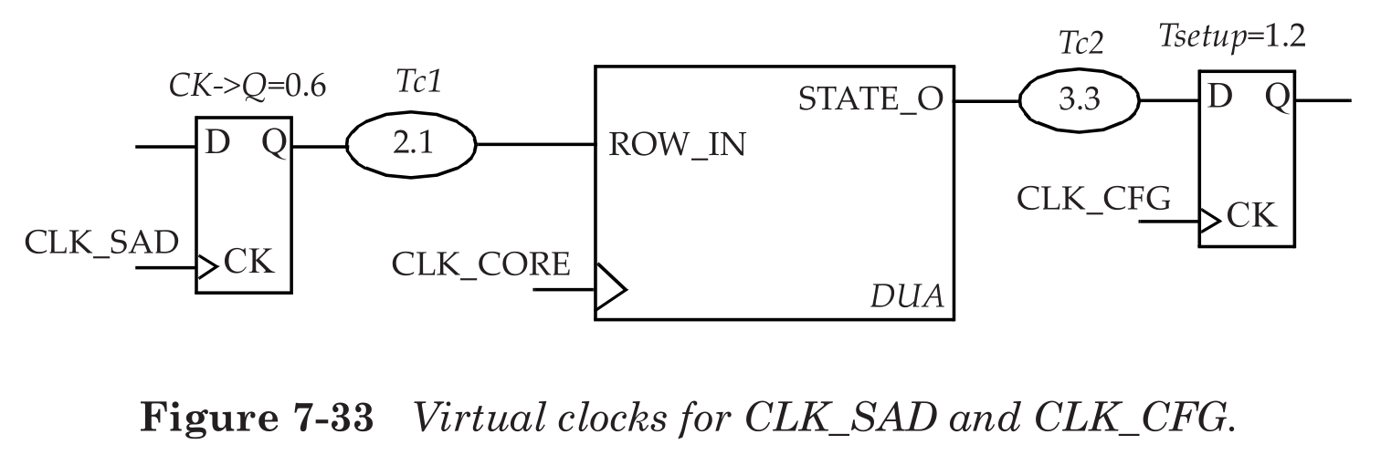
具体定义示例
1 | |
- 通过虚拟时钟可以更好的约束时序路径
6.7 Refining the Timing Analysis
四条精细化的STA分析路径,如果这个乱设容易让时序复杂了,因此需要对时序需求timepass属性进行分析:
- set_case_analysis: Specifies constant value on a pin of a cell, or on an input port.
- set_disable_timing: Breaks a timing arc of a cell.
- set_false_path: Specifies paths that are not real which implies that these paths are not checked in STA.
- set_multicycle_path: Specifies paths that can take longer than one clock cycle
1)set_case_analysis
芯片正常工作时DFT(test)是不要求工作的,因此需要关闭DFT(test)模式。
In a design, certain signals have a constant value in a specific mode of the chip.
For example, if a chip has DFT logic in it, then the TEST pin of the chip should be at 0 in normal functional mode. It is often useful to specify such constant values to STA
- test和normal两种模式的时钟选择:
 、
、
- 具体约束写法
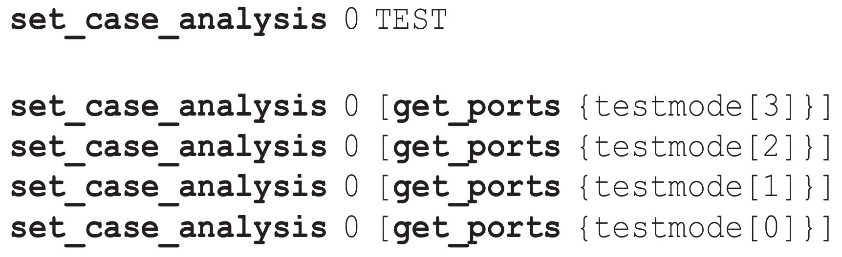
引脚不固定时,按情况具体约束
Another common application of case analysis is when the design can run on multiple clocks, and the selection of the appropriate clock is controlled by multiplexers. To make STA analysis easier and reduce CPU run time, it is beneficial to do STA for each clock selection separately.
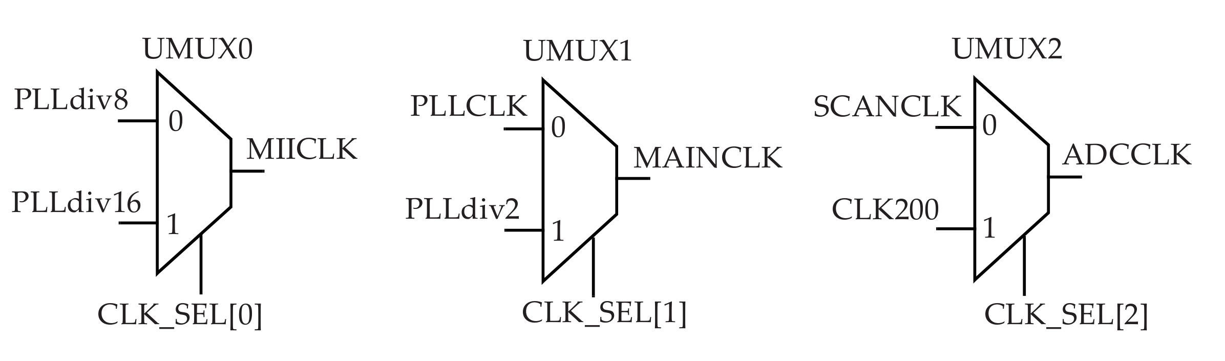
1 | |
2)set_disable_timing
意思:这不是一条时序路径,节点之间没有time pass,不进行STA分析,减少PT时间
In some situations, it is possible that a certain path through a cell cannot occur.
Such a timing arc can be broken by using the set_disable_timing SDC command
1 | |
3)set_false_path 伪路径
与disable区别:
- disable没有timing arc
- false根本不是一条时序路径
使用场景:
- 两个异步电路之间,由A时钟域->B时钟域中所有的路径不进行分析
- 有很多路径做逻辑简化时发现,有些时序路径永远不会出现时
1 | |
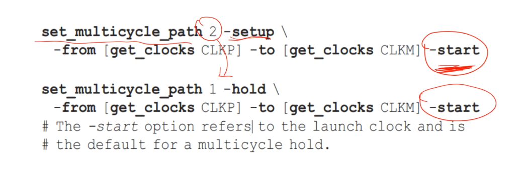
4)set_multicycle_path 多周期
使用场景:
- 在一个高延迟的路径下,提示PT这里要多个周期,别每个周期都检查
1 | |
6.8 补充
以上所有内容会以SDC脚本的形式出现,因此需要掌握SDC脚本的书写方法
一定要参考《DC命令手册》《PT命令手册》
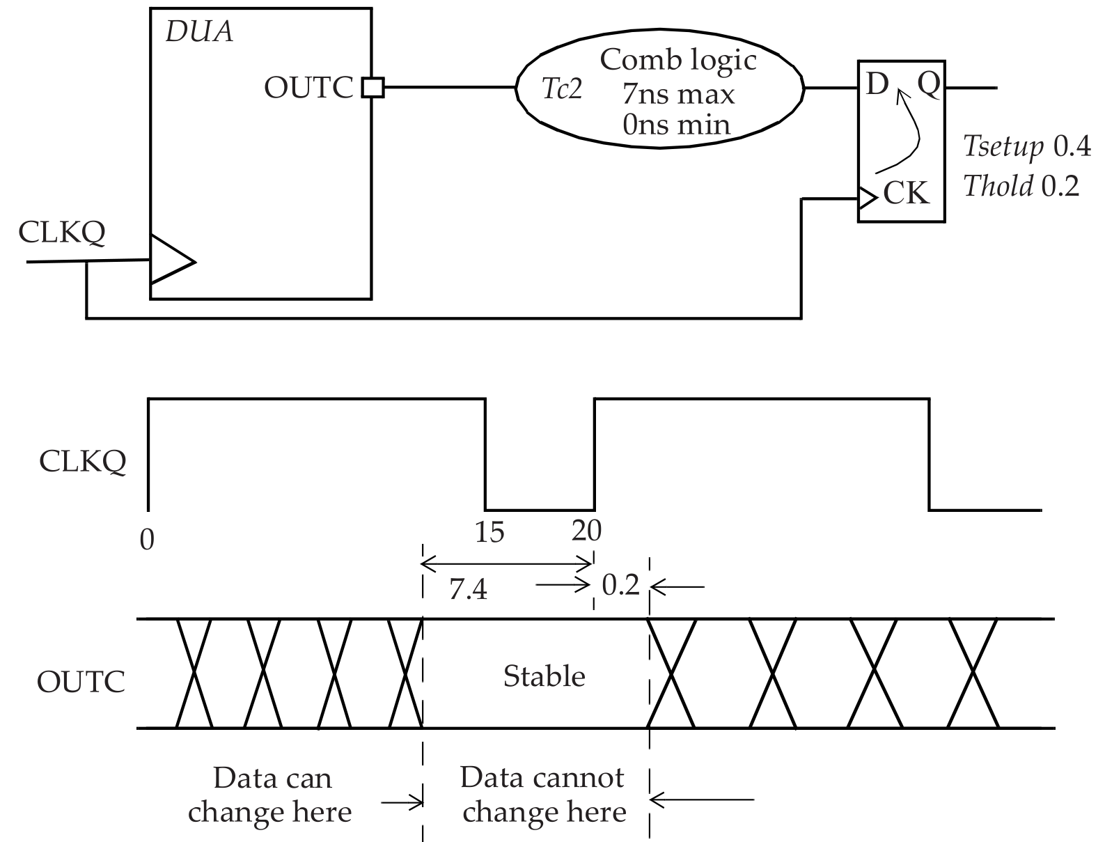
7 Timing Verification(一) 时序检查
- setup time check 建立时间的检查
- holdup time check 保持时间的检查
7.1 建立时间的检查
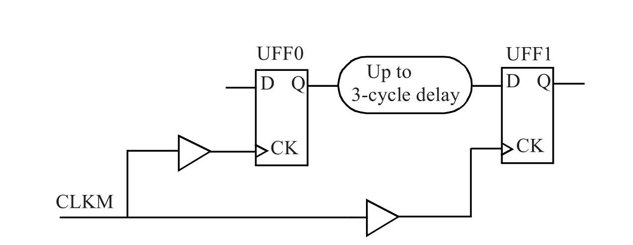
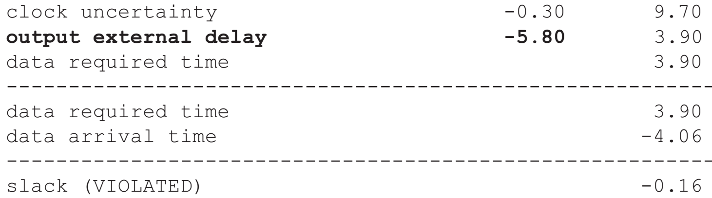
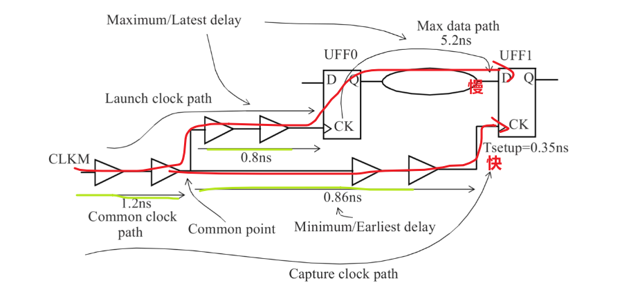
常见路径举例(有两条):
- 最常见路径上面的路径(Tlaunch+Tck2q+Tdp):UFF0.CK——UFF1.D
- capture路径下面的路径(CLKM的延迟):CLKM——UFF1.CK
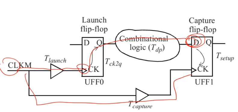
1)如何分析setup time是否满足要求
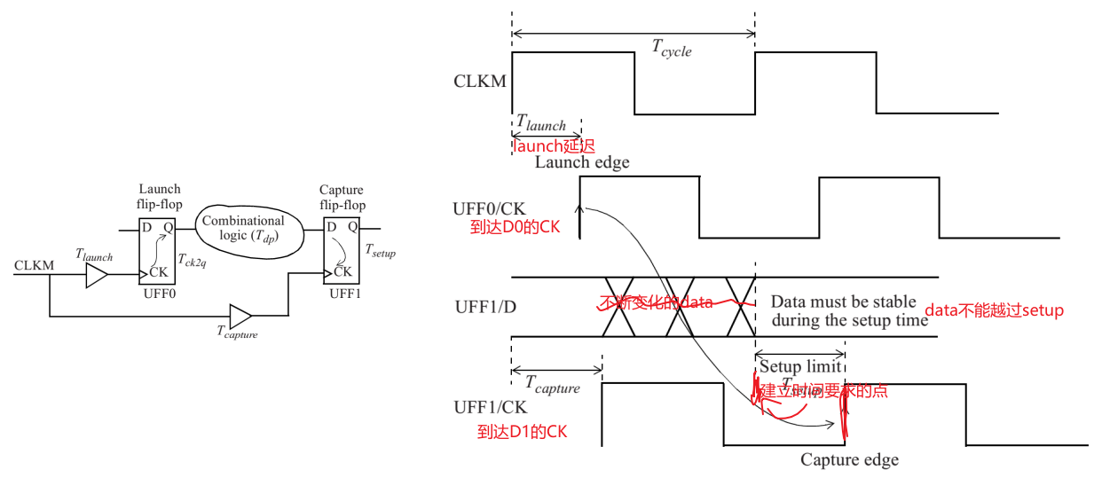
- launch路径
- capture路径
setup检查的公式表达:
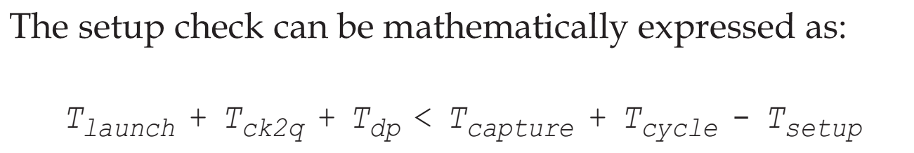
- 第一条launch路径的延迟小于第二条capture路径
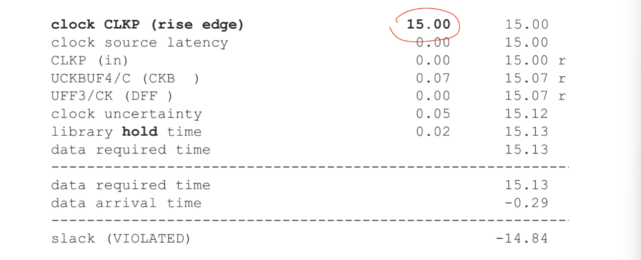
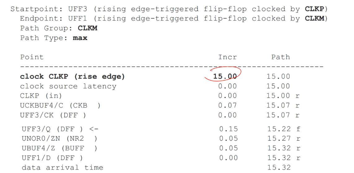
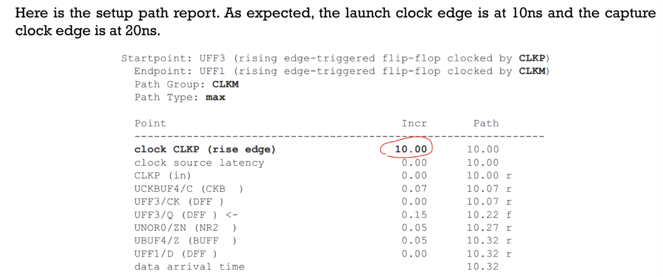
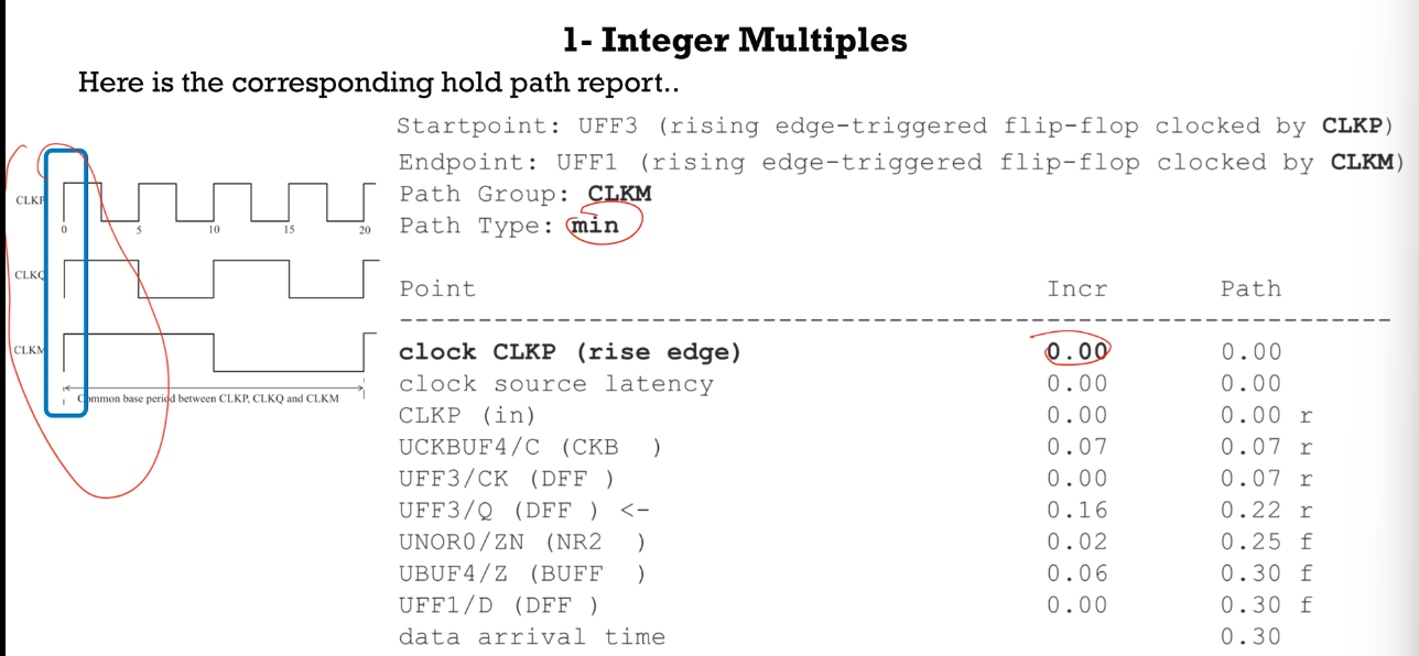
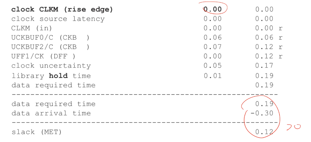
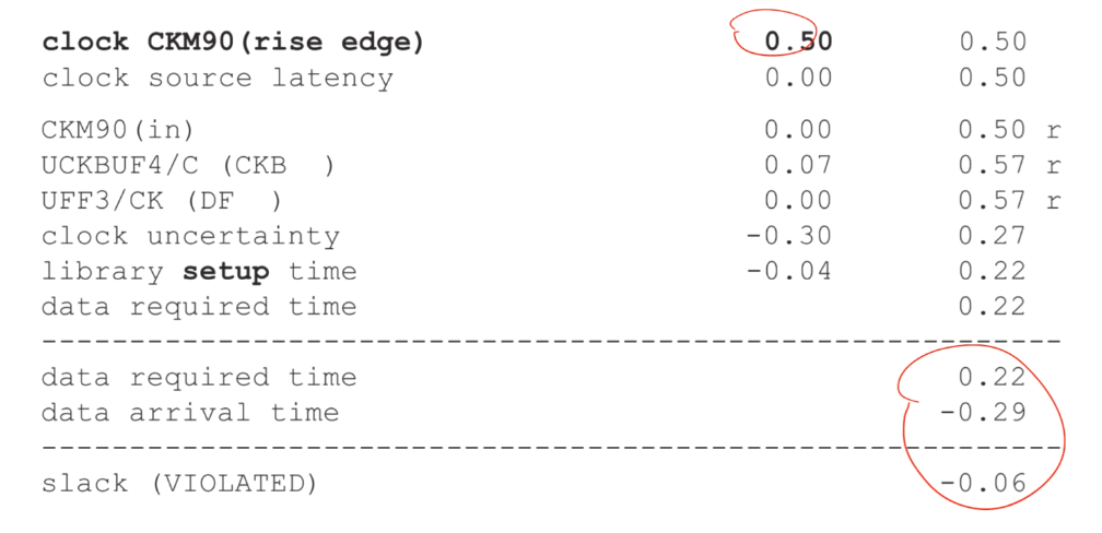
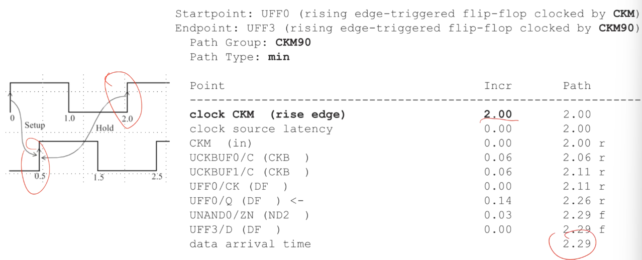
2)timing report讲解①(reg2reg/ff2ff)
timing report产生来源:DC/PT(后端的工具)
Flip-flop to Flip-flop Path
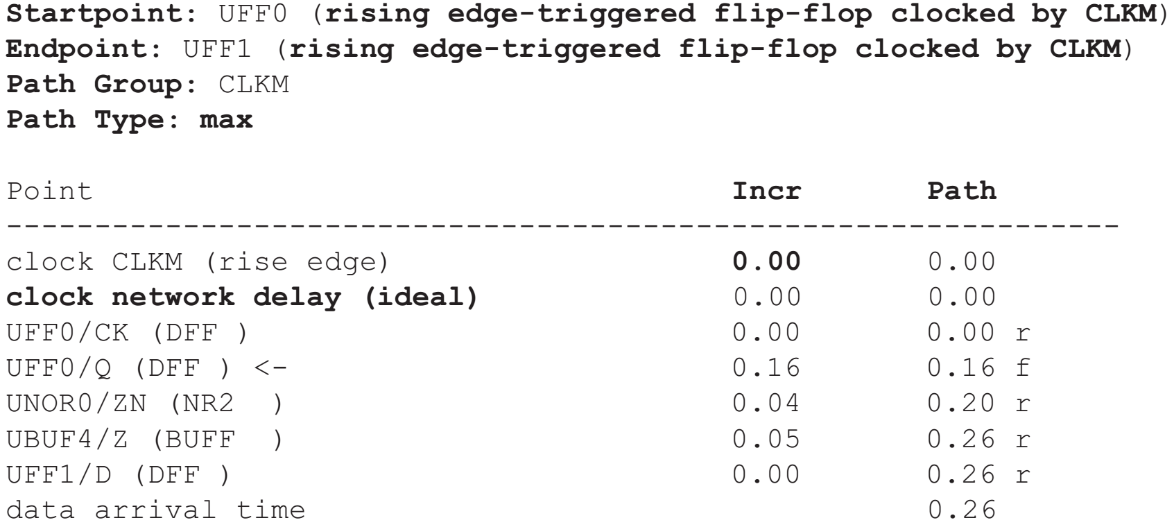
- 起点UFF0,被CLKM上升沿触发
- 重点UFF1,被CLKM上升沿触发
- 时钟组:根据终点是哪个CLK划分
- 极限max:Tlaunch时间最长时,依然小于Tcaputer建立时间
- Point:时序经过的每一个点
- Incr每个点自己的延迟
- Path从起点开始累计延迟值
- r/f:上升/翻转
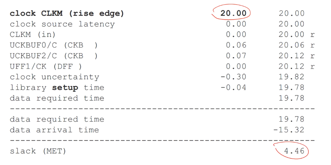
- data arrival time:数据到达时间(最终时间)
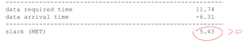
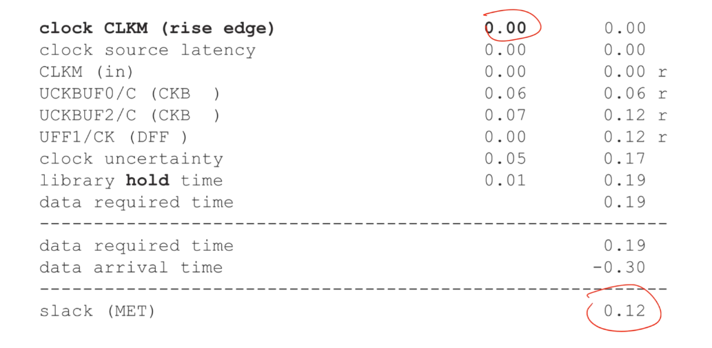
Ponit
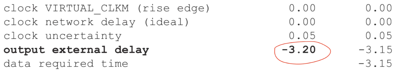
clock uncertainty:时钟误差,增加了表明更加严苛
data required time:数据要求到达时间
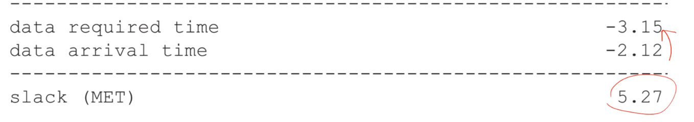
data required time - data arrival time >= 0 则满足setup公式满足要求
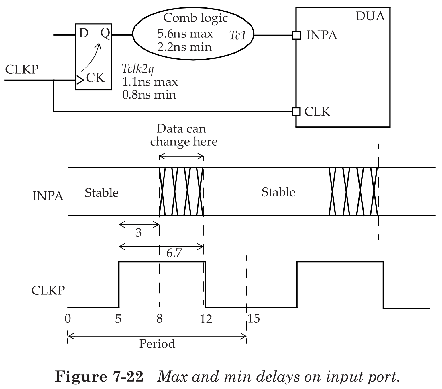
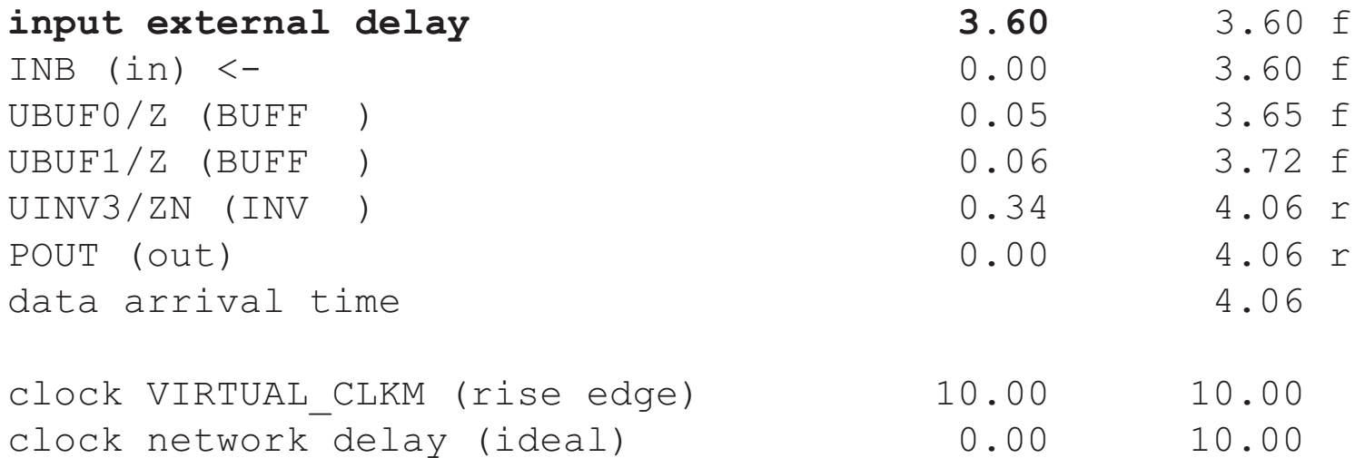
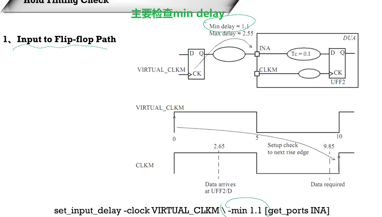
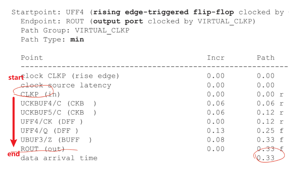
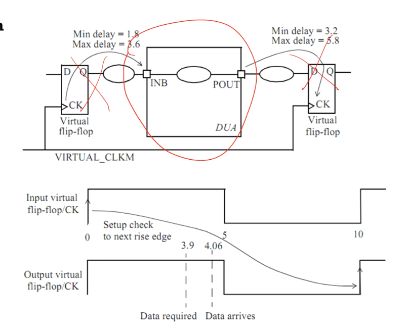
3)timing report讲解②(input port to register)
timing report产生来源:DC/PT(后端的工具)
Input to Flip-flop Path
- 上面提到过,增加Input Delay,两种Delay
- min delay
- max delay
Path
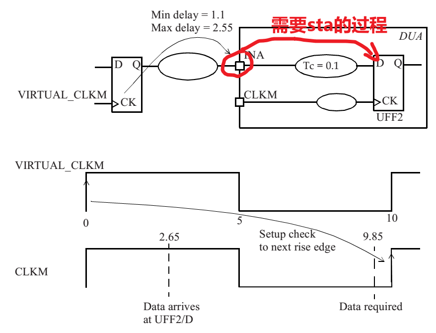
Constrain:
1 | |
timing report:
- launch path
- clock CLKP(虚拟时钟,延时为0)
- click network delay(虚拟时钟,延时为0)
- input external delay:自己加的,input port的延迟开始时额外延迟
- CIN:路径开始
- UFFD:路径终点
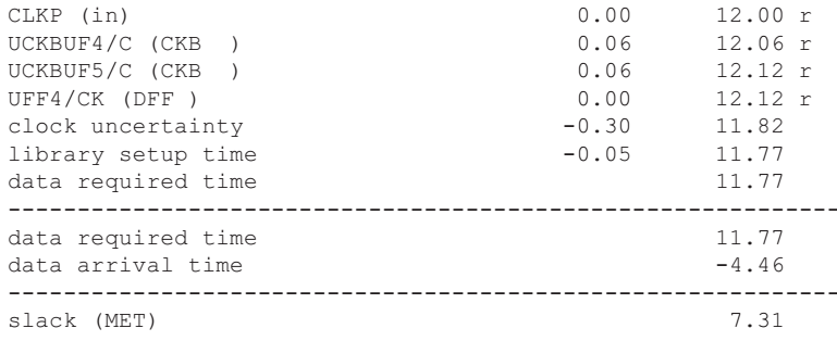
- capture path
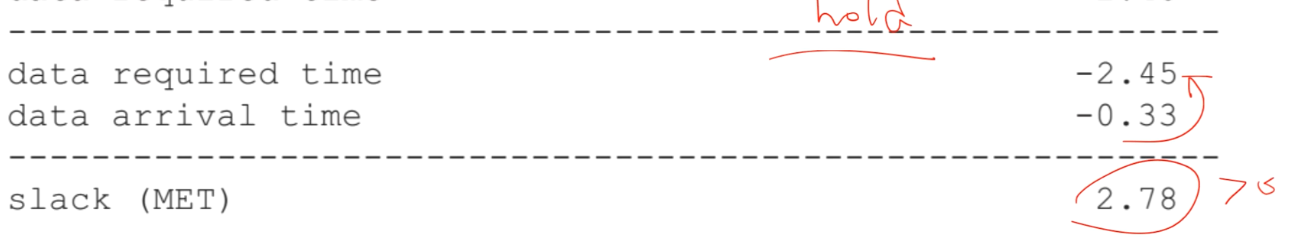
结果>=0则就满足
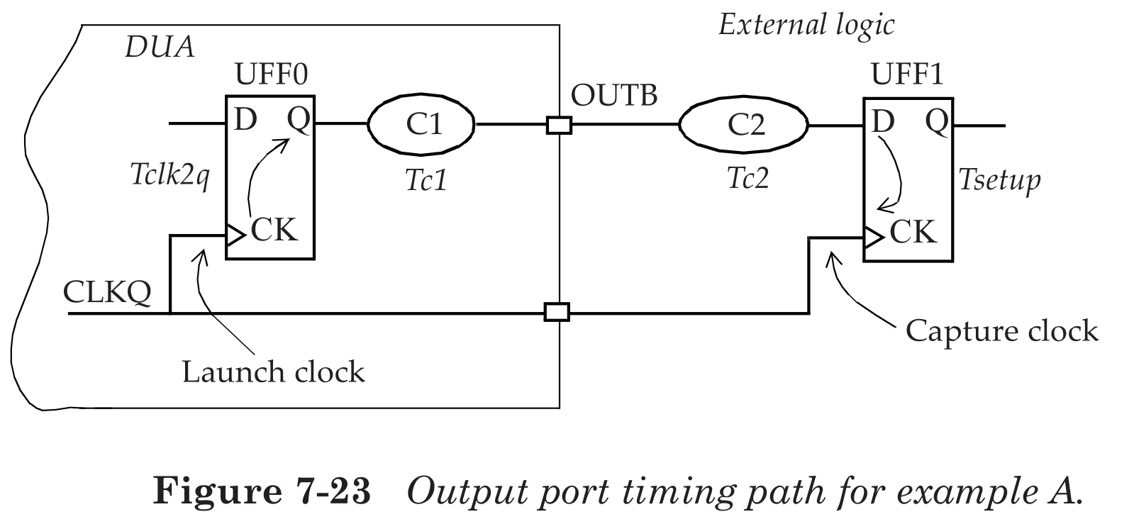
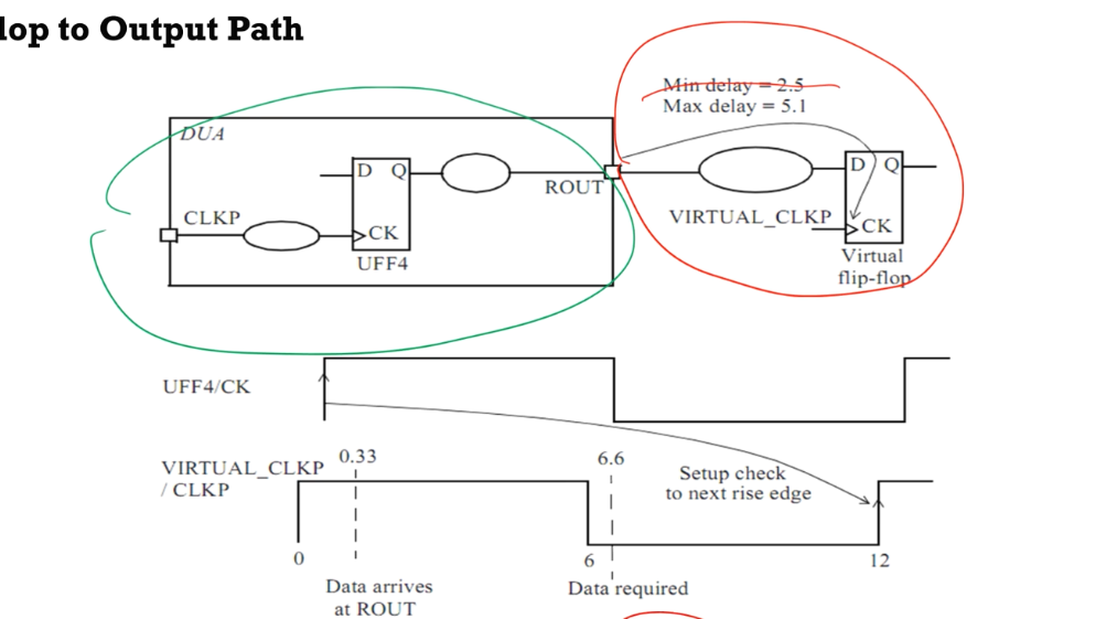
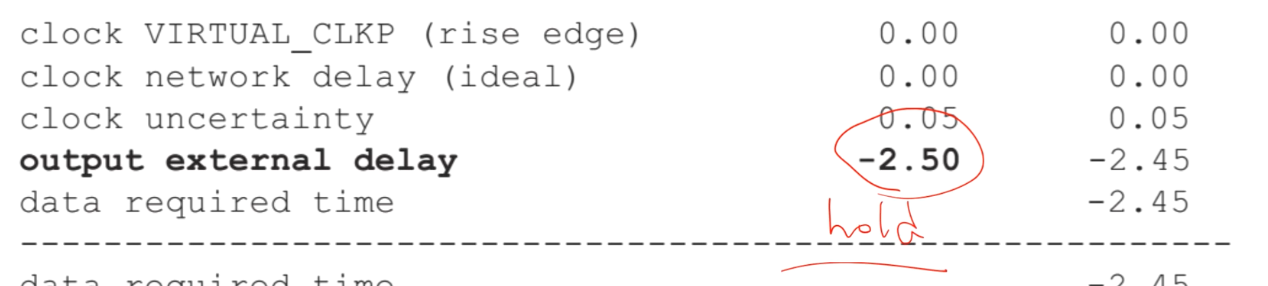
4)timing report讲解③(register to output port)
Flip-flop to Output Pat
- 与Input port to ff类似,区别在于除了约束output delay后还需约束load(set_load),这样才能确定最后一个cell的延迟值
Contrainst Code
1 | |
Path

Report

- launch path
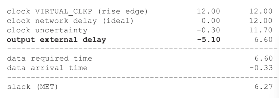
- capture path
- output external delay:增加的output delay(input port 的timing report加在了launch路径中)
sta、output delay位置示意
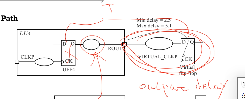
- CK->Q不关系
- output->虚拟时钟->D:output delay
- Q->output:sta部分
5)timing report讲解④(input to output path)
Path

sta 位置示意

TCL Code
1 | |
Report
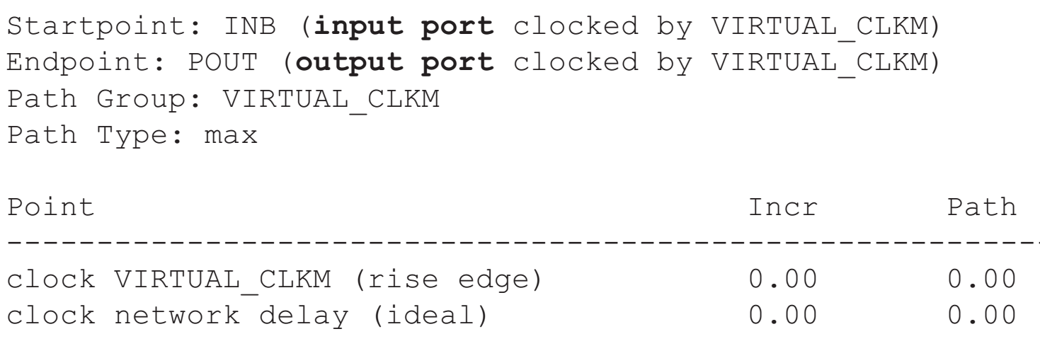
- 注意这里小于0,需要考虑如何修改
7.2 保持时间的检查
1)如何分析holdup time是否满足要求
同setup
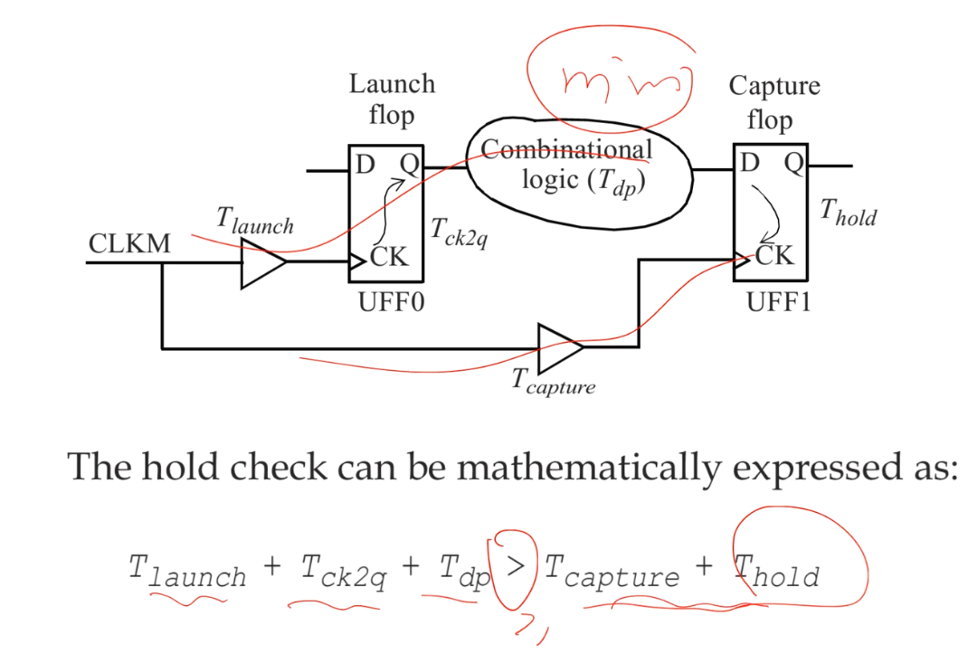
Just like the setup check, a hold timing check is between the launch flipflop - the flip-flop that launches the data, and the capture flip-flop - the flip-flop that captures the data and whose hold time must be satisfied.
The clocks to these two flip-flops can be the same or can be different.
与setup区别
check在同一边缘
The hold check is from one active edge of the clock in the launch flip-flop to the same clock edge at the capture flip-flop
回忆一下触发器基础概念就懂了,而setup的capture与launch差了一个周期
hold check独立时钟,与时钟区域没有关系
a hold check is independent of the clock period
The hold check is carried out on each active edge of the clock of the capture flip-flop
2 Paths:
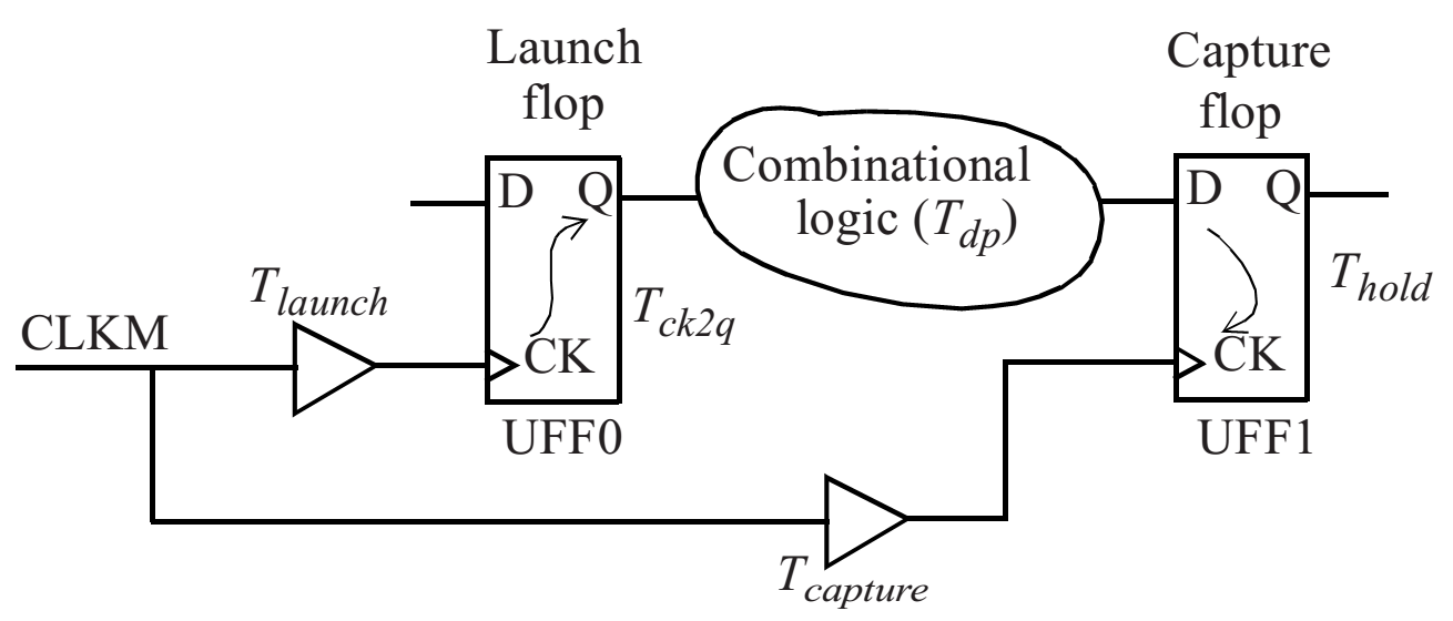

- launch路径
- capture路径
公式表达
- 极限情况:左边(launch time)的最小值>右边(capture time)的最大值
- 区别于setup:
- setup查看launch time的最大值
- hold查看launch time的最小值
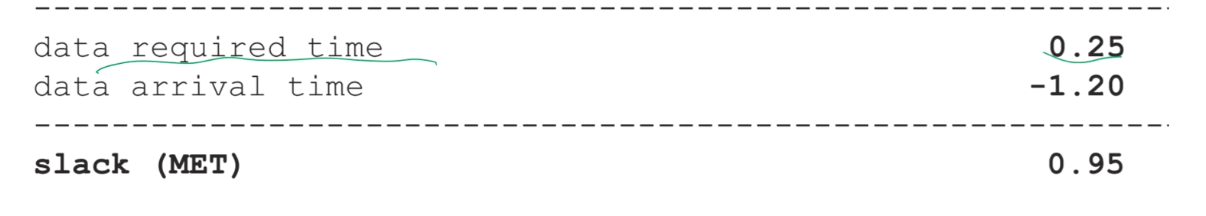
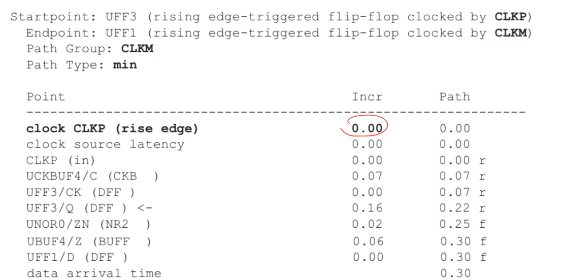
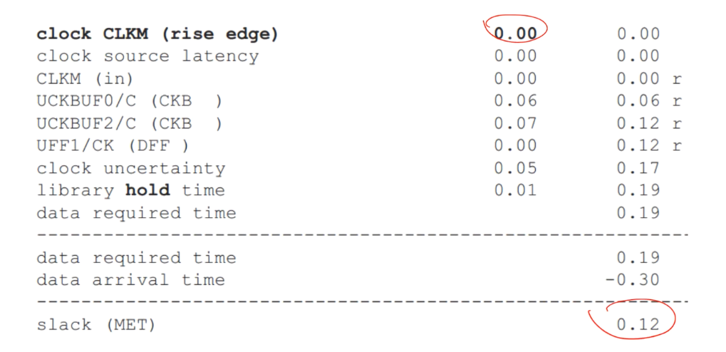
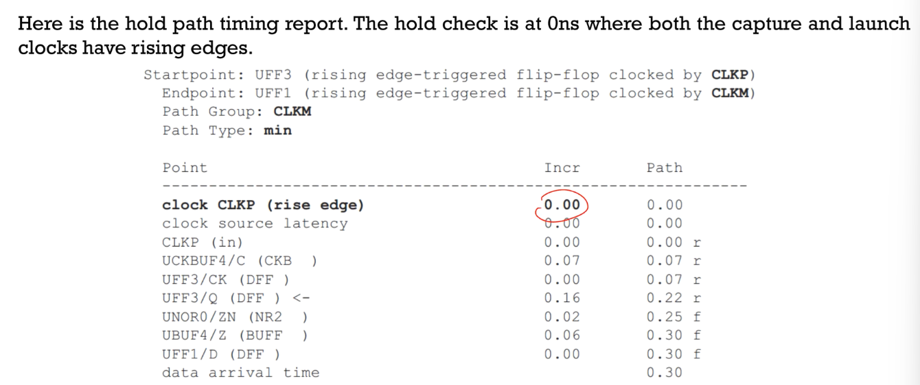
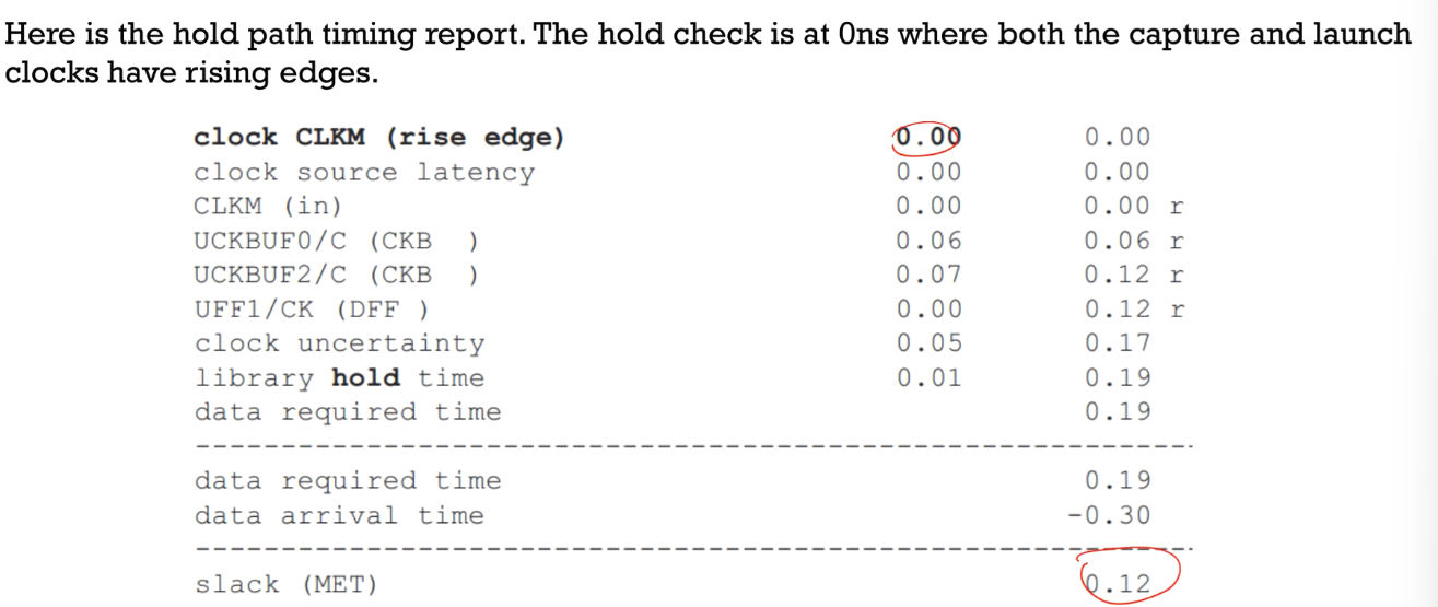
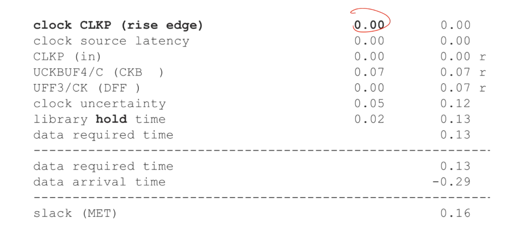
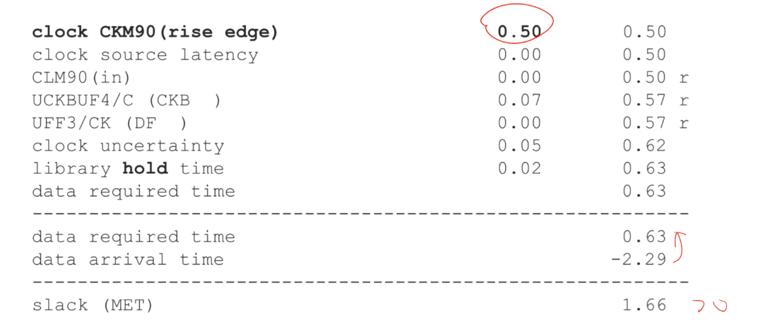
2)timing report讲解①(reg2reg/ff2ff)
Report
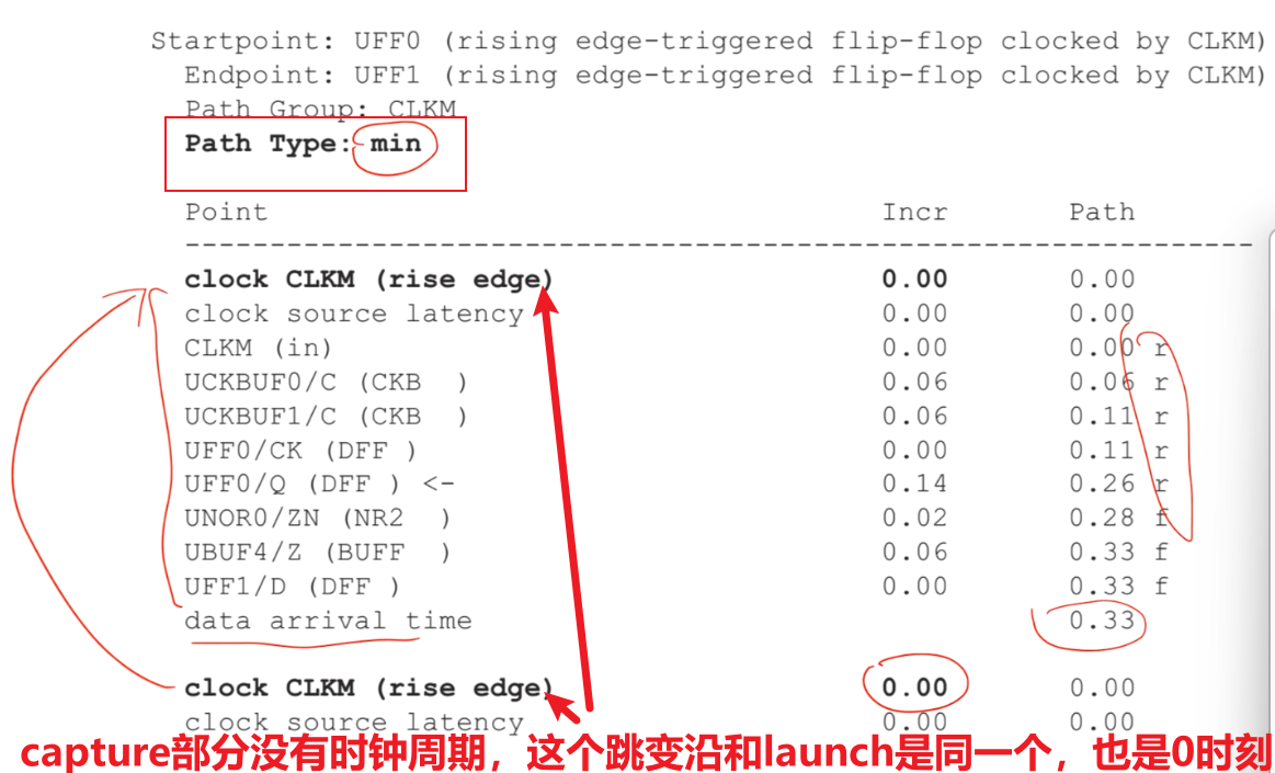
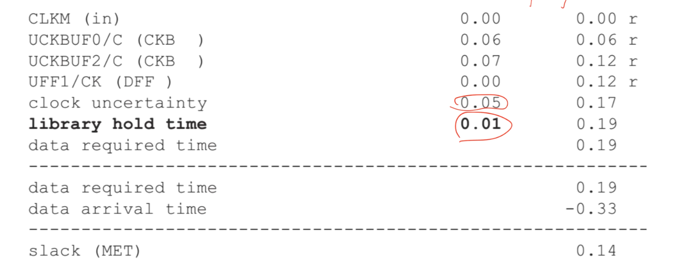
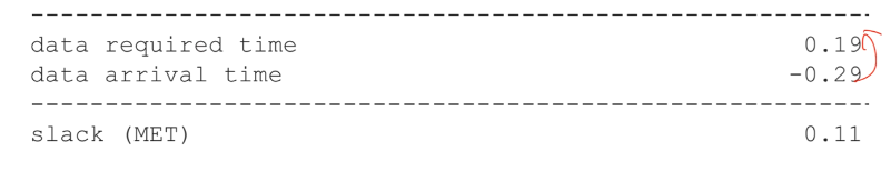
要点
- Path Type:min,对应上一节提到的查看最小值
- clock uncertainty:是正值,要往前(在setup时是负值)
- data required time 0.19:
- required time比arrival time小
- slack:EDA为了保持与setup体验一致性,此处位置为arrival time - required time
- 区别于setup中required time-arrival time
3)timing report讲解②(input port to register)
Path
TCL Code
1 | |
Report(圈出的是设置的值)

- launch path
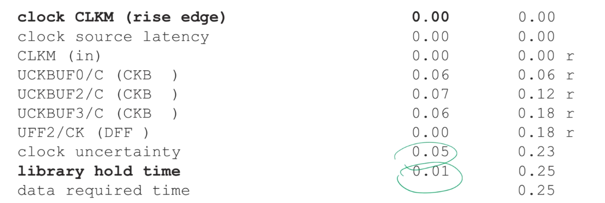
- capture path
- 结果
4)timing report讲解③(register to output port)
Path
TCL Code
1 | |
Report(圈出的是设置的值)
- launch path
- capture path
- 结果
5)timing report讲解④(input to output path)
Path
TCL Code
1 | |
Report(圈出的是设置的值)

- launch路径
- input delay
- capture路径
- output delay
- 结果
7.3 总结
setup:

Launch路径<=Capture路径
Factors:
- Tlaunch:launch的时钟网络延迟
- Tck2q:ck到q的延迟
- Tdp:logic延迟
- Tcapture:capture的时钟网络
- Tcycle:一个时钟周期
- Tsetup:一个setup
Analysis:
- Tdp:combinational一般是我们自己写的,因此STA不满足的时候也只能对此进行修改,需要保证次值最大时公式成立
- 时钟网络之间的延迟一般都很小
- Tcycle:给定的
- Tsetup:工艺库中
holdup time:
8 Timing Verification(二) 多周期半周期伪路径检查
- Multicycle Paths 多周期路径
- Half-Cycle Paths 半周期路径
- False Paths 伪周期路径
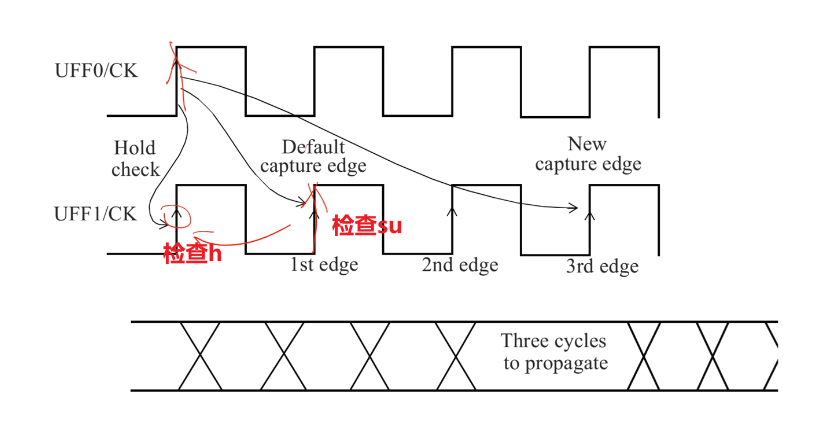
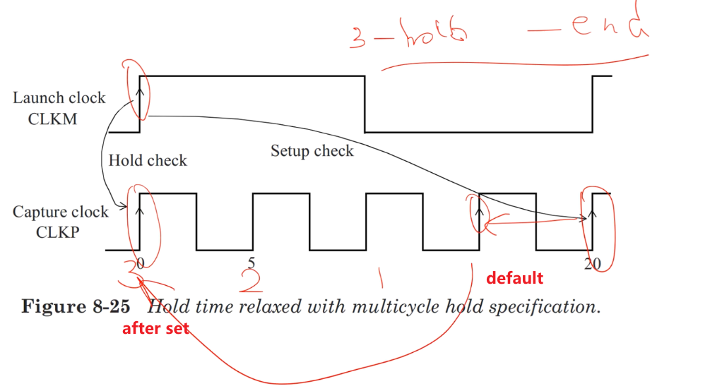
8.1 Multicycle Paths 多周期路径
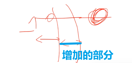
概述:
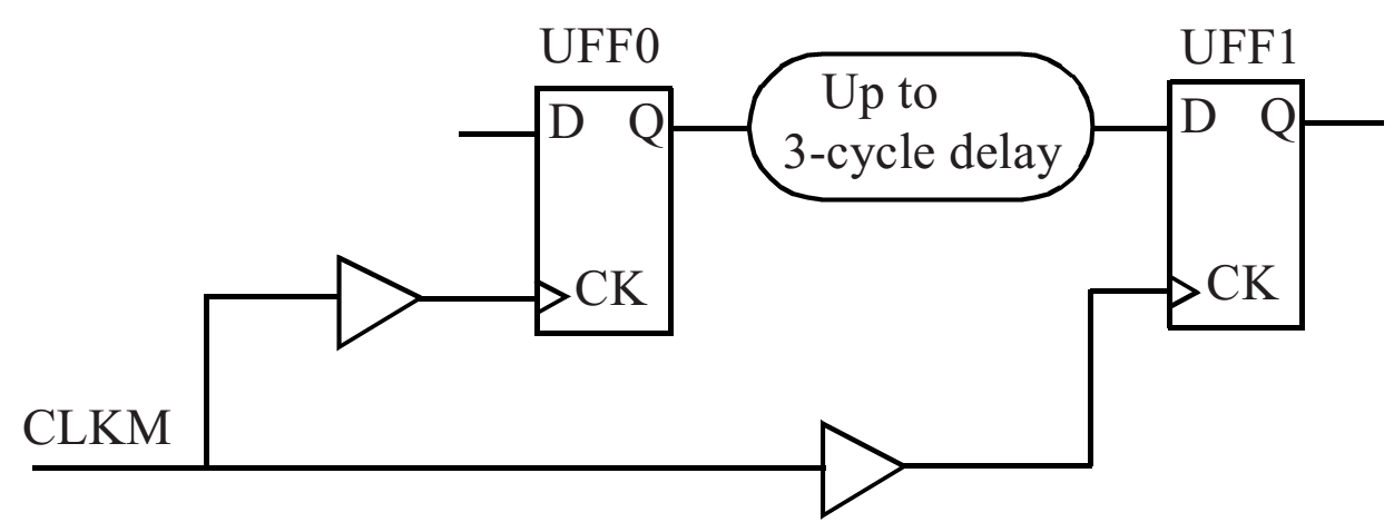
Up to 3-cycle delay时传统的STA无法满足要求
In some cases, the combinational data path between two flip-flops can take more than one clock cycle to propagate through the logic. In such cases, the combinational path is declared as a multicycle path. Even though the data is being captured by the capture flip-flop on every clock edge, we direct STA that the relevant capture edge occurs after the specified number of clock cycles
约束代码
Since the data path can take up to three clock cycles, a setup multicycle check of three cycles should be specified.
The multicycle setup constraints specified to achieve this are given below:
- 针对setup的一个3周期时钟路径约束设置
1 | |
单周期的setup,hold检查
- setup检查如图所示
- hold检查要往前推一个周期
三周期的setup检查:

- setup检查
Report
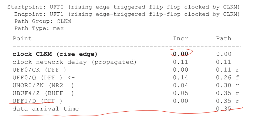
- Launch
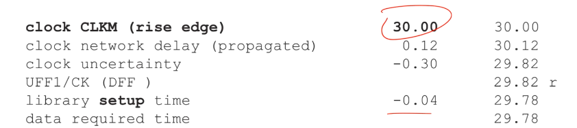
- Capture
- clock CLKM是三个周期,所以是30
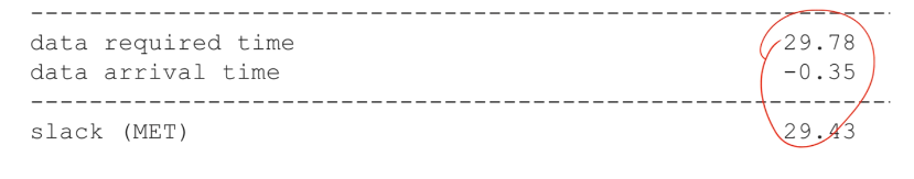
- 结果
三周期hold检查:
- N周期setup需要被一个N-1周期的hold获取
In most designs, a multicycle setup specified as N (cycles) should be accompanied by a
multicycle hold constraint specified as N-1 (cycles)
约束代码:
1 | |
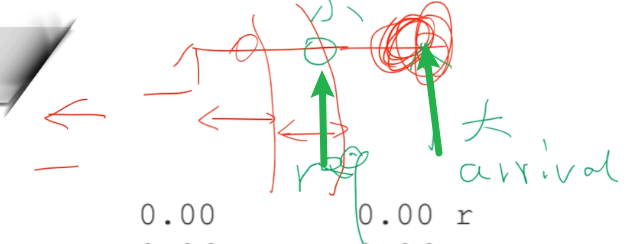
默认,提前的hold时序路径

- 使用指令后hold check从default提前了两个周期
Report

- Launch
- min:hold check

- Capture
- clock CLKP往前移动了两个周期到了0
- 结果
对比一下默认没加约束的3周期hold检查

Report

capture&结果
- clock CLKM是两个周期的
- hold time非常大
- slack远远不满足要求
总结
多周期一定要设置
- setup具体第N个时钟
- hold为N-1提前
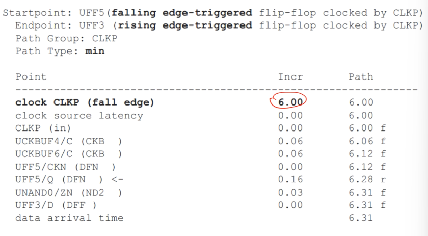
8.2 Half-Cycle Paths半周期
触发器的出发边缘不一样(有的是下降沿有的是上升沿,会造成半周期的情况)
If a design has both negative-edge triggered flip-flops (active clock edge isfalling edge) and positive-edge triggered flip-flops (active clock edge is rising edge), it is likely that half-cycle paths exist in the design.
Setup Graph
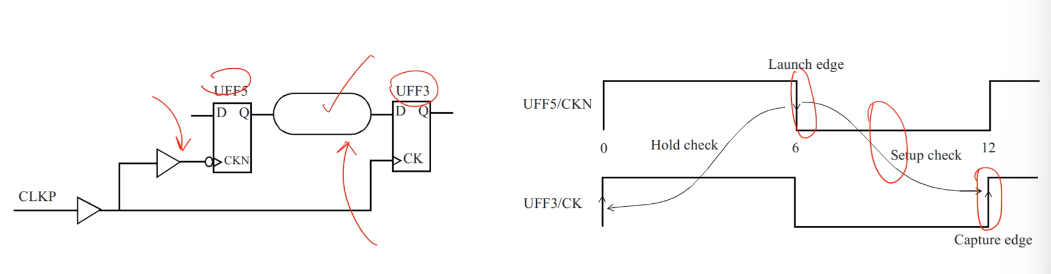
- UFF5时钟上升沿
- UFF3时钟下降沿
- 两个触发器之间只剩下半个周期,给逻辑的时间也只剩下半个周期
Setup Report
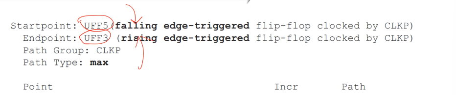
- attribution
- Startpoint:下降沿
- Endpot:上升沿

- Launch
- clock CLKP是从下降沿6ns开始的(周期是12ns)
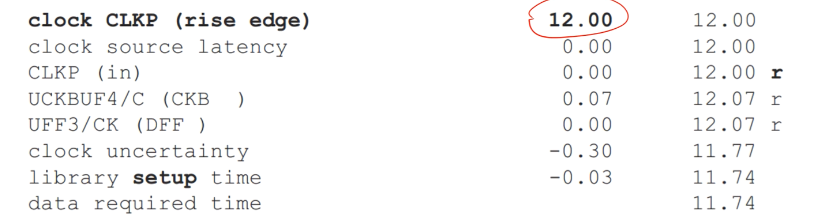
- Capture
- clock CLKP是12ns
- 结果
Hold Timing Graph & Report
While the data path gets only half-cycle for setup check, an extra half-cycle is available for the hold timing check. Here is the hold timing path
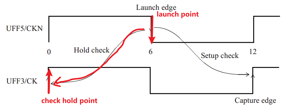
- Launch

- Capture
- 结果
- 一开始就是6
- slack很轻松的就满足了
- 半周期特性
- 半周期使用场景:A->B传输数据的时候用半周期更稳妥
- 特点:
- setup非常紧(只剩T/2)
- 数字电路的特点:setup违例了非常好修,hold违例了不容易修,因此半周期使得处理STA不容易特别棘手
- hold非常松
- setup非常紧(只剩T/2)
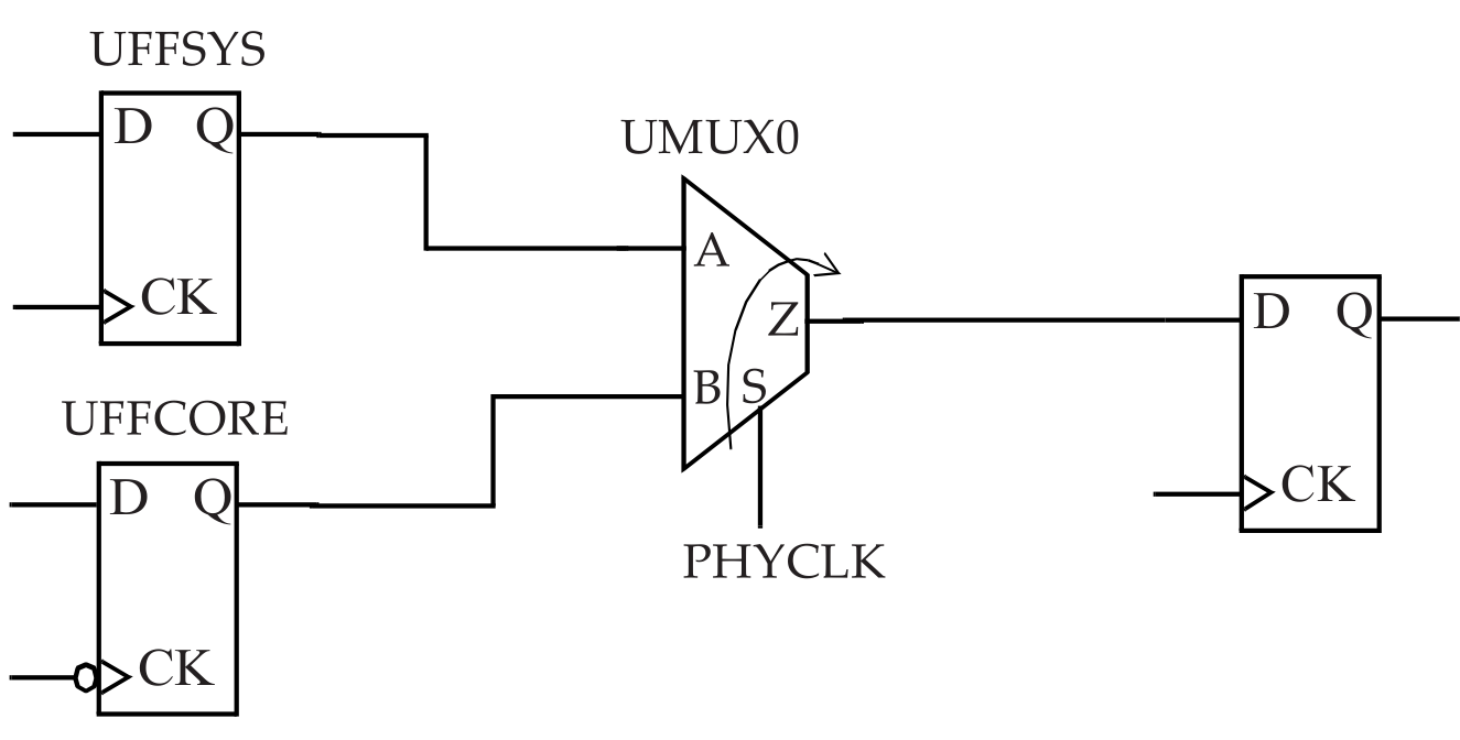
8.3 False Paths伪路径
It is possible that certain timing paths are not real (or not possible) in the actual functional operation of the design.
Such paths can be turned off during STA by setting these as false paths.
A false path is ignored by the STA for analysis
伪路径:
- 电路中不可能存在/发生的。我们需要告诉EDA工具这种路径不会发生,从而提高STA准确性,降低STA计算使得跑的更快
伪路径通常发生在:
- 异步跨时钟域
- 一个常量路径(如一个很复杂的逻辑电路,推导下来却是常量)
STA中如何处理伪路径
- 直接指定某一路径
When a false path is specified through a pin of a cell, all paths that go through that pin are ignored for timing analysis.
The advantage of identifying the false paths is that the analysis space is reduced, thereby allowing the analysis to focus only on the real paths.
This helps cut down the analysis time as well.
However, too many false paths using the through specification can slow down the analysis(太多的约束有时候不一定会减小STA时间,而会增大)
Code
1 | |
- SCAN和CORE是什么?
大部分电路会有两个时钟:SCAN(DFT时)、CORE(正常模式),所以我们会对从SCAN,CORE时钟出来的路径进行伪路径忽略
- UMUX0/S
任何一个满足情况的时钟都是startpoint

定义伪路径应尽可能精确
-though参数不推荐
尽可能少使用-though参数,除非特别有必要的时候
Another recommendation is to minimize the usage of through options, as it adds unnecessary runtime complexity.
The -through option should only be used where it is absolutely necessary and there is no
alternate way to specify the false path.
别把多周期路径给设成伪路径
- 一定要把真的虚假路径设为虚假路径,不要随意设
From an optimization perspective, another guideline is to not use a false path when a multicycle path is the real intent.
If a signal is sampled at a known or predictable time, no matter how far out, a multicycle path specification should be used so that the path has some constraint and gets optimized to meet the multicycle constraint.
If a false path is used on a path that is sampled many clock cycles later, optimization of the remaining logic may invariably slow this path even beyond what may be necessary.
Report
- Launch
- Capture
- 结果
9 Timing Verification(三) 多时钟域,多时钟分析
(注意)本节提到的都是同步时钟,异步时钟不是这种表现形式
- Timing across Clock Domains
- Multiple Clocks
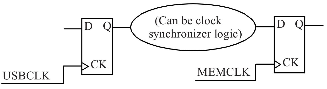
9.1 Timing across Clock Domains多时钟域分析
1)slow to fast clock domains
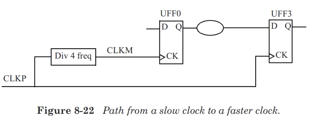
- Div 4 freq四分频
对上述电路进行静态时序分析
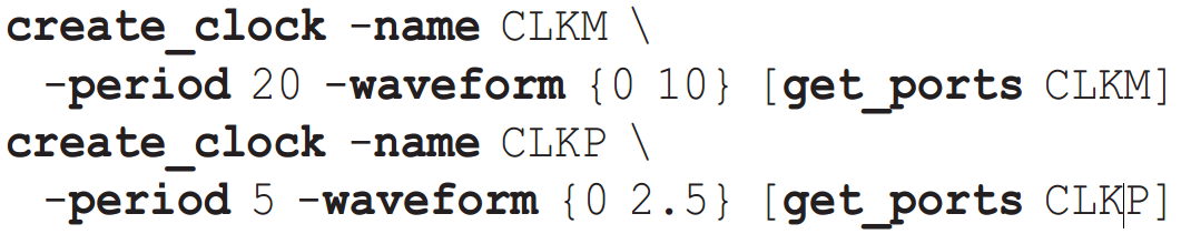
Graph & Code
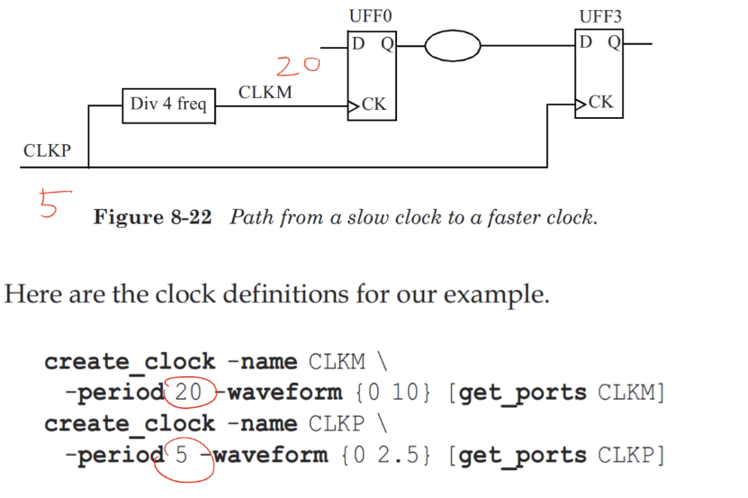
- 分别把时钟定义为20和5周期
Wave
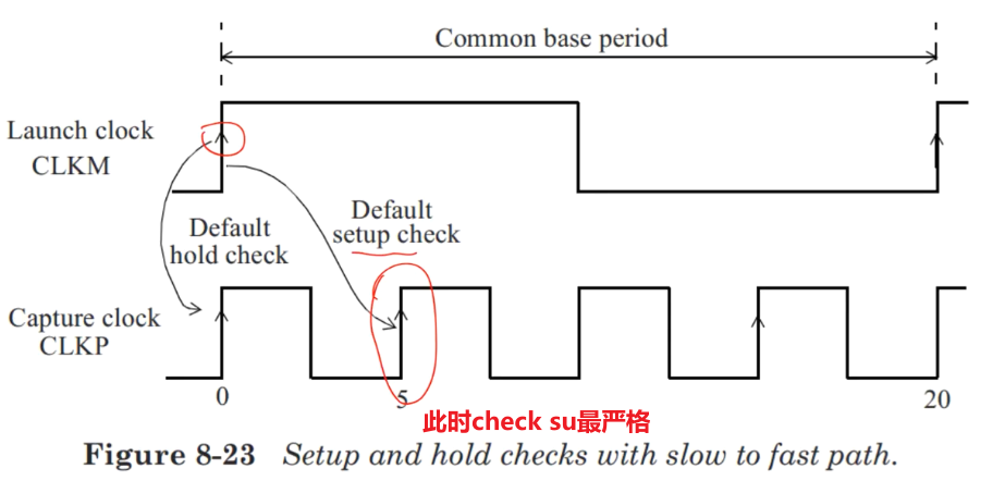
- 我们在最严格的情况下进行分析
By default, the most constraining setup edge relationship is used, which in this case is the very next capture edge. Here is a setup path report that shows this.
- CLKM发送数据,CLKP接收数据
- 从慢时钟到块时钟
Report
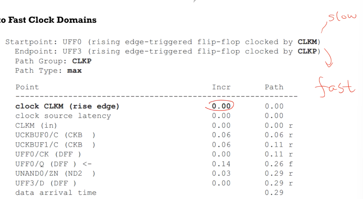
- Launch
- Capture
Hold Check
使用多周期约束对setup进行检查(合理)
- 使用多周期约束对不是特别严苛,但对hold check来说不太合理
In the above example, we can see that the launch data is available every fourth cycle of the capture clock. Let us assume that the intention is not to capture data on the very next active edge of CLKP, but to capture on every 4th capture edge. This assumption gives the combinational logic between the flip-flops four periods of CLKP to propagate, which is 20ns. We can do this by setting the following multicycle specification:
1 | |
- 一定要注意加到end上,也就是要有-end参数

这样的话可以把时间拉长到四个周期,中间是组合逻辑,相对合理
Report
上述情况的hold检查(不合理)
Figure 8-24 shows the hold check - note that the hold check is derived from the setup check and defaults to one cycle preceding the intended capture edge.
Here is the hold timing report. Notice that the hold capture edge is at 15ns, one cycle prior to the setup capture edge.
- Report

使用多周期约束对hold进行检查(合理)
In most designs, this is not the intended check, and the hold check should be moved all the way back to where the launch edge is.We do this by setting a hold multicycle specification of 3.
1 | |
- 往回退三个周期,保证check点在0ns
The cycle of 3 moves the hold checking edge back three cycles, that is, to time 0ns.
The distinction with a setup multicycle is that in setup, the setup capture edge moves forward by the specified number of cycles from the default setup capture edge; in a hold multicycle, the hold check edge moves backward from the default hold check edge (one cycle before setup edge)
总结
In summary, if a setup multicycle of N cycles is specified, then most likely a hold multicycle of N-1 cycles should also be specified
- 给setupN,给holdN-1
2)fast to low clock domains
In this subsection, we consider examples where the data path goes from a fast clock domain to a slow clock domain. The default setup and hold checks are as shown in Figure 8-26 when the following clock definitions are used.
时钟定义
Graph

正常的时序逻辑检查(不太合理)
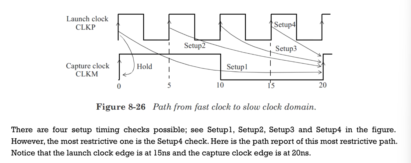
正常情况的hold检查(不合理暴漏了出来)
不合理的原因
Similar to the setup checks, there are four hold checks possible.
Figure 8-26 shows the most restrictive hold check which ensures that the capture edge at 0ns does not capture the data being launched at 0ns.
Here is the timing report for this hold check.
使用多周期约束进行合理设置
In general, a designer may specify the data path from the fast clock to the slow clock to be a multicycle path. If the setup check is relaxed to provide two cycles of the faster clock for the data path, the following is included for this multicycle specification:
- 起点是快的,因此需要换成start
check点移动以后
In this case, Figure 8-27 shows the clock edges used for the setup and hold checks. The -start option specifies that the unit for the number of cycles (2 in this case) is that of the launch clock (CLKP in this case). The setup multicycle of 2 moves the launch edge one edge prior to the default launch edge, that is, at 10ns instead of the default 15ns. The hold multicycle ensures that the capture of the earlier data can reliably occur at 0ns due to the launch edge also at 0ns.

- launch 往后
- hold往前,还是0
Report
- setup
- hold
- launch,capture都是从0开始
3)总结
start和end选项
Unlike the case of paths from slow to fast clock domains, a good rule of thumb for multi-frequency multicycle path specification in the case of paths from fast to slow clock domains is to use the -start option. The setup and hold checks are then adjusted based upon the fast clock
9.2 Multiple Clocks多时钟
- 多时钟之间是整数倍关系
- 多时种之间是非整数的关系
- 相位移动情况
1)整数倍时钟
我们使用公共时钟进行STA
Often there are multiple clocks defined in a design with frequencies that are simple (or integer) multiples of each other.
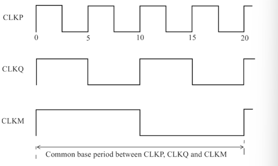
In such cases, STA is performed by computing a common base period(公共周期) among all related clocks (two clocks are related if they have a data path between their domains).
The common base period is established so that all clocks are synchronized.
时钟定义
- 定义了三个不同频率的时钟
- 20(公共周期),10,5
1 | |
从最快时钟(CLKP)到最慢时钟(CLKM)的分析
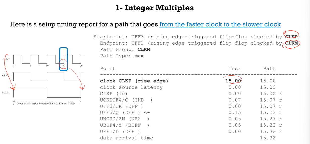

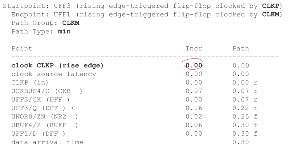
- 最严苛的情况:CLKP(15ns)——>CLKM(20ns)
hold check:都是从0开始
2)非整数倍时钟
倍频不是整数倍
时钟5/8
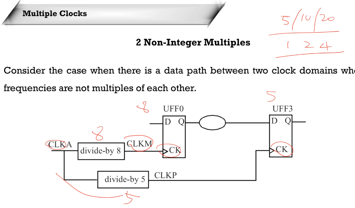
三个时钟的约束的定义
1 | |
公共时钟选取
- 取存在数据交互的时钟的最小公倍数对STA进行处理
- 可以方便的查看哪个沿发送、哪个沿接收
The timing analysis process computes a common period for the related clocks, and the clocks are then expanded to this base period.
Note that the common period is found only for related clocks (that is, clocks that have timing paths between them).
Graph(从CLKM到CLKP时)
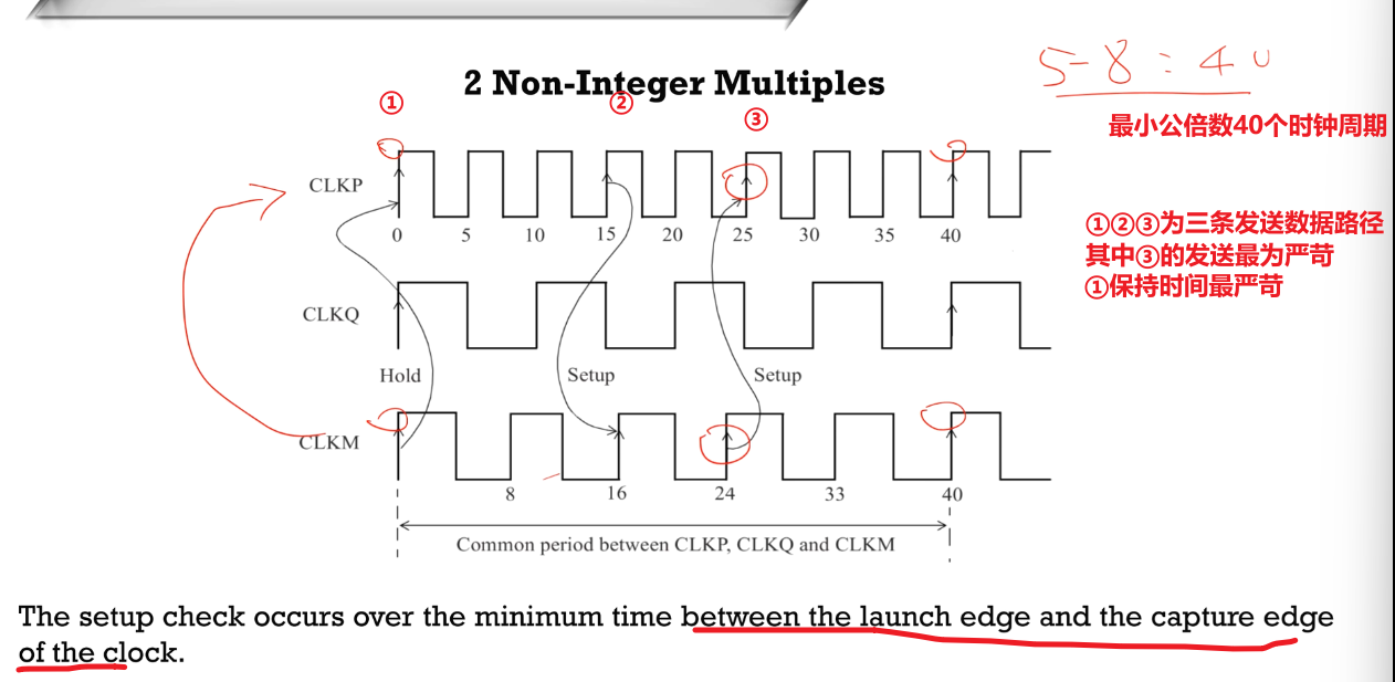
- 找到最严苛的setup路径(最短的时候)
- 找到最严苛的hold路径(最长的时候)
Report
- 建立时间


- 保持时间检查

Graph(从CLKP到CLKM时)
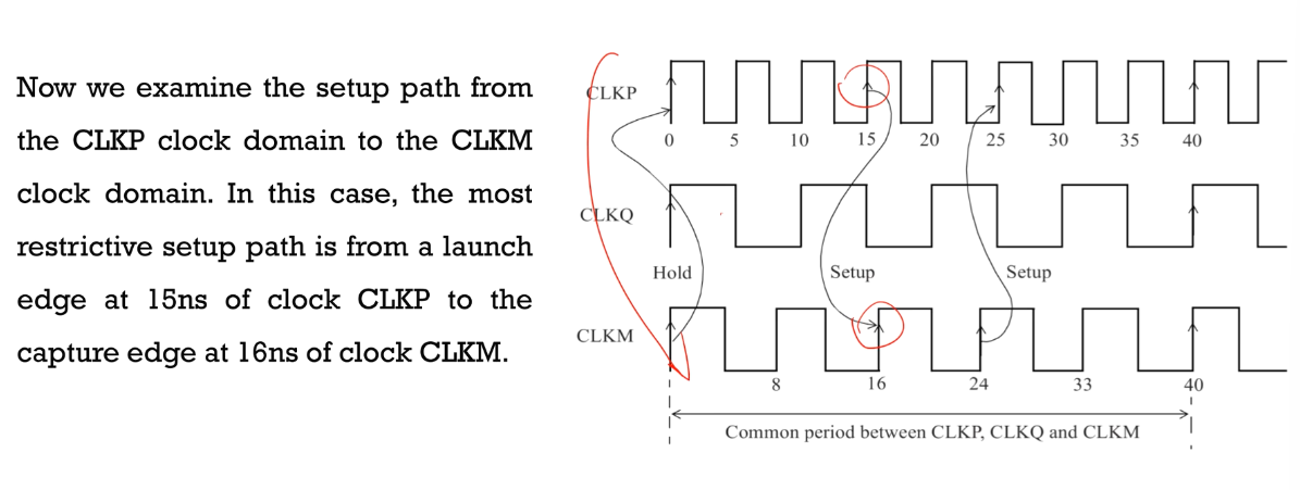
- 找到最严苛的setup路径(最短的时候)
- 找到最严苛的hold路径(最长的时候)
Report
- setup
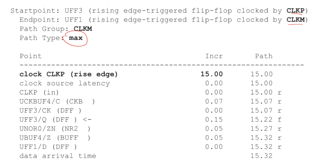

- hold
3)Phase Shifted 相位移动(频率相同)
一个两时钟相位偏移90°的例子
- 类似半周期的例子
- 对hold友好,对setup不友好
两时钟约束定义
1 | |
Graph & Wave
- 默认check point
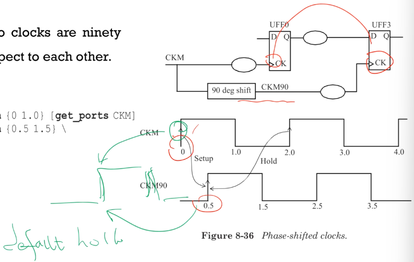
- 为了方便查看check points都往迁移一个周期
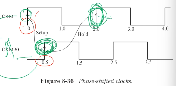
Report
- setup
- 比较难满足
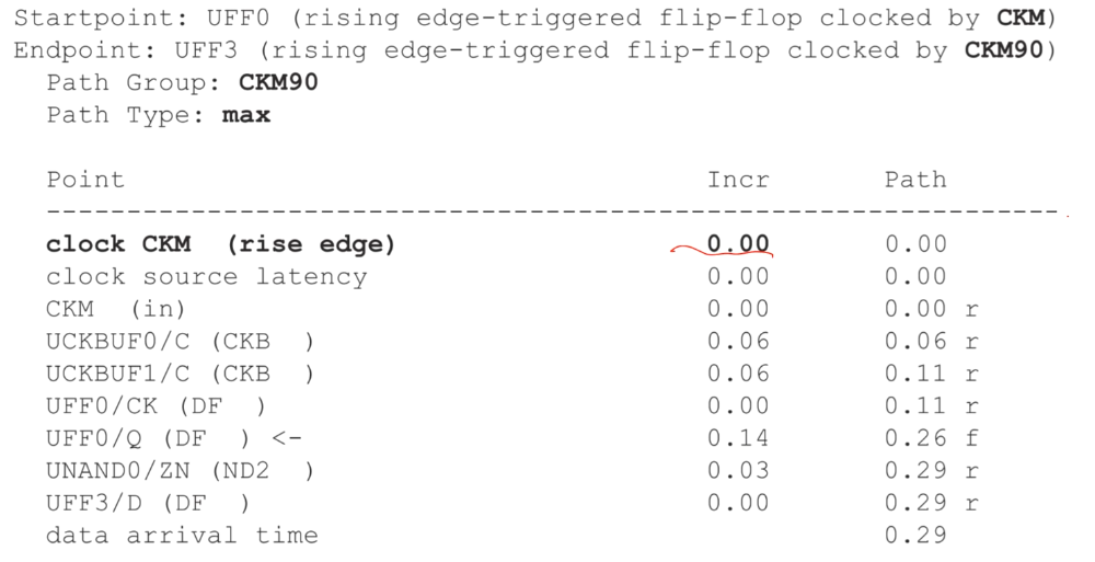
- hold
10 Robust Verification鲁棒性检查
On-Chip Variations
Setup time check
Hold time check
10.1 On-Chip Variations
由于工艺的不同,片上不同区域延迟可能不同
In general, the process and environmental parameters may not be uniform across different portions of the die.
Due to process variations, identical MOS transistors in different portions of the die may not have similar characteristics. These differences are due to process variations within the die.
通常是这五个因素产生:
- IR drop variation along the die area affecting the local power supply.
- Voltage threshold variation of the PMOS or the NMOS device.
- Channel length variation of the PMOS or the NMOS device.
- Temperature variations due to local hot spots.
- Interconnect metal etch or thickness variations impacting the interconnect resistance or capacitance.
上述PVT因素通常被称为OCV(On-Chip Variations,片上偏差),通常来说这些偏差对wire和cell延迟都有影响
The PVT variations described above are referred to as On-Chip Variations (OCV) and these variations can affect the wire delays and cell delays in different portions of the chip.
我们需要在STA中加入这些因素的影响效果,通常来说是对一些路径进行放大或缩小的形式(加入delay的形式)
Since the clock and data paths can be affected differently by the OCV, the timing verification can model the OCV effect by making the PVT conditions for the launch and capture paths to be slightly different.
The STA can include the OCV effect by derating the delays of specific paths, that is, by making those paths faster or slower and then validating the behavior of the design with these variations.
The cell delays or wire delays or both can be derated to model the effect of OCV.
10.2 OCV设置(setup)

- 由于OCV的存在使得实际中三个路径延迟都不一样
- 最严苛的情况:最长的路径特别慢,最短的路径特别快;导致数据到达特别慢,采样时钟特别快,如下图所示
- 我们需要把OCV的最严苛情况提现到STA中,具体把某一部分放大或缩小
 公式回顾
公式回顾
整体公式: LaunchClockPath + MaxDataPath <= ClockPeriod +CaptureClockPath - Tsetup_UFF1
单独看时钟周期:This implies that the minimum clock period = LaunchClockPath + MaxDataPath - CaptureClockPath + Tsetup_UFF1
理想情况下的时序分析
考虑OCV的情况
1 | |
The derating factors apply uniformly to all net delays and cell delays.
If an application scenario warrants different derating factors for cells and nets, the -cell_delay and the -net_delay options can be used in the set_timing_derate specification.
setup hold具体怎么做
- setup
- 对于long path(如data path/launch clock)使其更大,乘以1.n
- 对于shor path(如capture clock)使其更小,乘以0.n
- hold
- 对于long path(如data path/launch clock)使其更小,乘以0.n,让数据比较短
- 对于shor path(如capture clock)使其更大,乘以1.n,让时钟网络更靠后
Long path delays (for example, data paths and launch clock path for setup checks or capture clock paths for hold checks) are multiplied by the derate value specified using the -late option.
Short path delays (for example, capture clock paths for setup checks or data paths and launch clock paths for hold checks) are multiplied by the derate values specified using the -early option.
If no derating factors are specified, a value of 1.0 is assumed
示例约束后

- 频率变低,对组合电路更严格,需要减小组合逻辑延迟,需要对组合逻辑优化
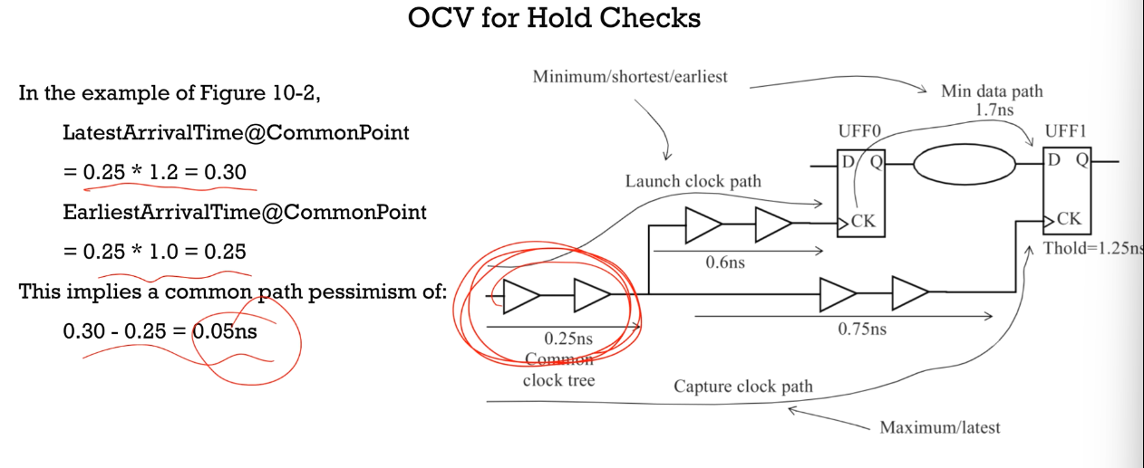
10.3 CPP(Common Path Pessimism)问题
- 背景:我们对launch和capture的公共路径同时放大缩小了
- 带来了悲观设置
Applying different derating for the launch and capture clock is overly
pessimistic as in reality this part of the clock tree will really be at only one PVT condition, either as a maximum path or as a minimum path (or anything in between) but never both at the same time.
- CPP与CPPR
- CPP(Common Path Pessimism)
- CPPR(Common Path Pessimism Removal)/CRPR(Clock Reconvergence Pessimism Remova),移除CPP的方法
The pessimism caused by different derating factors applied on the common part of the clock tree is called Common Path Pessimism (CPP) which should be removed during the analysis.
CPPR, which stands for Common Path Pessimism Removal, is often listed as a separate item in a path report. It is also labeled as Clock Reconvergence Pessimism Removal (CRPR).
CPPR具体实现
CPP = LatestArrivalTime@CommonPoint - EarliestArrivalTime@CommonPoint
- 找公共路径上插值最大的两个值(period原始*(max_rate-min_rate))
CPPR is the removal of artificially induced pessimism between the launch clock path and the capture clock path in timing analysis.
If the same clock drives both the capture and the launch flip-flops, then the clock tree will likely share a common portion before branching.The common point is defined as the output pin of the last cell in the common portion of the clock tree.
CPPR示例
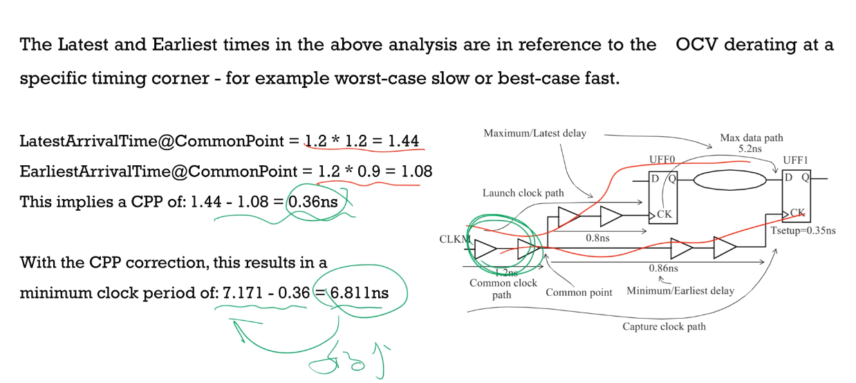
总结
Applying the OCV derating has increased the minimum clock period from 5.49ns to 6.811ns for this example design.
This illustrates that the OCV variations modeled by these derating factors can reduce the maximum frequency of operation of the design.
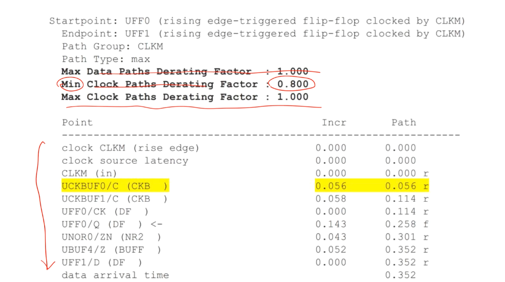
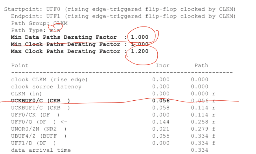
10.4 更严谨的设置倍数,提高OCV时的速度
OCV时已经时不合理了,因此我们需要加快检查速度
If the setup timing check is being performed at the worst-case PVT condition, no derating is necessary on the late paths as they are already the worst possible
However, derating can be applied to the early paths by making those paths faster by using a specific derating, for example, speeding up the early paths by 10%.
定义约束
A derate specification at the worst-case slow corner may be something like:
1 | |
这样做可以:使得STA更合理一点
- 比较差的路径,延迟不进行放大
- 比较好的路径(capture),延迟缩小变得更快
The above derate settings are for max path (or setup) checks at the worstcase slow corner; thus the late path OCV derate setting is kept at 1.0 so as not to slow it beyond the worst-case slow corner.
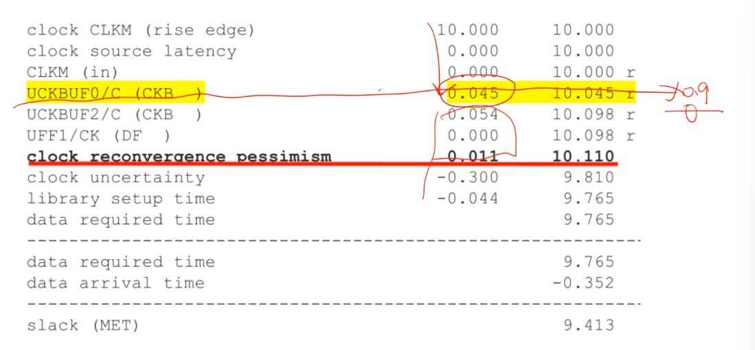
Here is the setup timing check path report performed at the worst-case slow corner. The derating used by the late paths are reported as Max Data Paths Derating Factor and as Max Clock Paths Derating Factor.
The derating used for the early paths is reported as Min Clock Paths Derating Factor.
Report
- 更严谨的设置倍数、CPPR设置
 总结
总结
The cell UCKBUF0 is on the common clock path, that is, on both the capture clock path and the launch clock path.
Since the common clock path cannot have a different derating, the difference in timing for this common path, 56ps - 45ps = 11ps, is corrected separately.
10.5 OCV设置(hold)
1)OCV
hold timing我们也要判断路径的快慢,通常来说:
- launch clock path and the data path,smallest delays
- capture clock path,largest delays
所以我们悲观角度来看,缩小launch,增大capture,使得数据往后移
If the PVT conditions are different along the chip, the worst condition for hold check occurs:
when the launch clock path and the data path have OCV conditions which result in the smallest delays, that is, when we have the earliest launch clock, and the capture clock path has the OCV conditions which result in the largest delays, that is, has the latest capture clock
公式回顾
LaunchClockPath + MinDataPath - CaptureClockPath - Thold_UFF1 >= 0
示例约束
- 正常计算
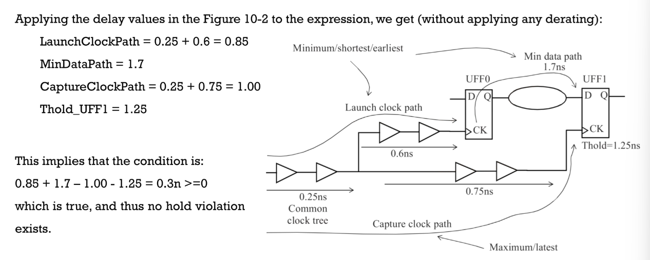
- 使用约束
1 | |

- 使用约束后的时序更差了,更不满足了
2)更严谨的设置倍数
hold time check快路径已经很快乐,我们需要将慢路径再慢一点
In general, the hold timing check is performed at the best-case fast PVT corner.
In such a scenario, no derating is necessary on the early paths, as those paths are already the earliest possible.
However, derating can be applied on the late paths by making these slower by a specific derating factor, for example, slowing the late paths by 20.
修改后的约束
1 | |
Report
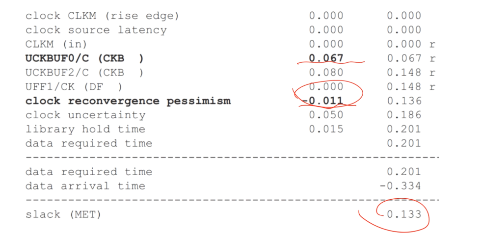
总结
Notice that the late paths are derated by +20% while the early paths are not derated. See cell UCKBUF0.
Its delay on the launch path is 56ps while the delay on the capture path is 67ps - derated by +20%.
UCKBUF0 is the cell on the common clock tree and thus the pessimism introduced due to different derating on this common clock tree is, 67ps - 56ps = 11ps, which is accounted for separately on the line clock reconvergence pessimism.
11 Time Borrowing/Cycle Stealing
11.1 回顾
Latch与DFF
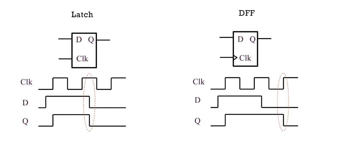
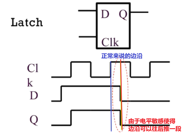
- Latch
- 有效电平内是透明的,无效电平时保存
我们之前分析的都是DFF,接下来分析Latch,time borrowing技术是对latch分析时使用到的特殊技术
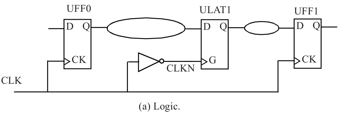
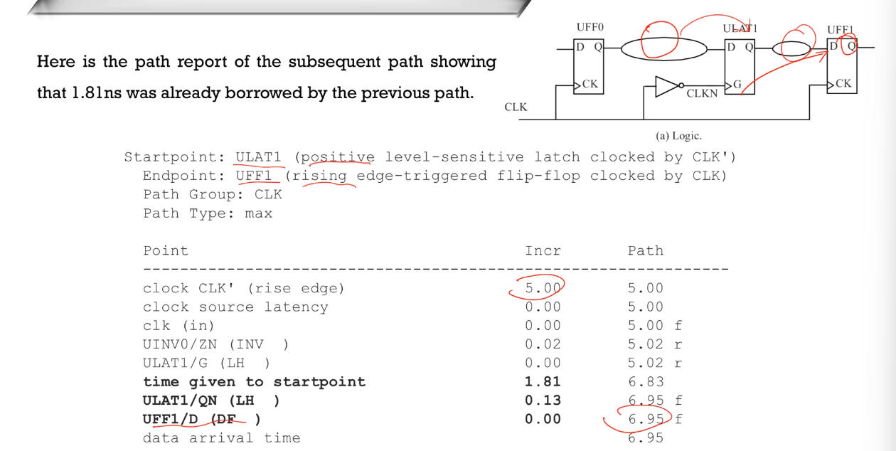
11.2 Time Borrowing
1)概念
opening edge & closing edge
The time borrowing technique, which is also called cycle stealing, occurs at a latch.
- 边缘跳变后时有效电平(In a latch, one edge of the clock makes the latch transparent, that is, it opens the latch so that output of the latch is the same as the data input; this clock edge is called the opening edge.)
- 边缘跳变后时无效电平(The second edge of the clock closes the latch, that is, any change on the data input is no longer available at the output of the latch; this clock edge is called the closing edge. )
通过opening edge & closing edge可以分析约束是什么样子
what is time borrowing(Latch的setup和hold)
Typically, the data should be ready at a latch input before the active edge of the clock.
However, since a latch is transparent when the clock is active, the data can arrive later than the active clock edge, that is, it can borrow time from the next cycle.If such time is borrowed, the time available for the following stage (latch to another sequential cell) is reduced
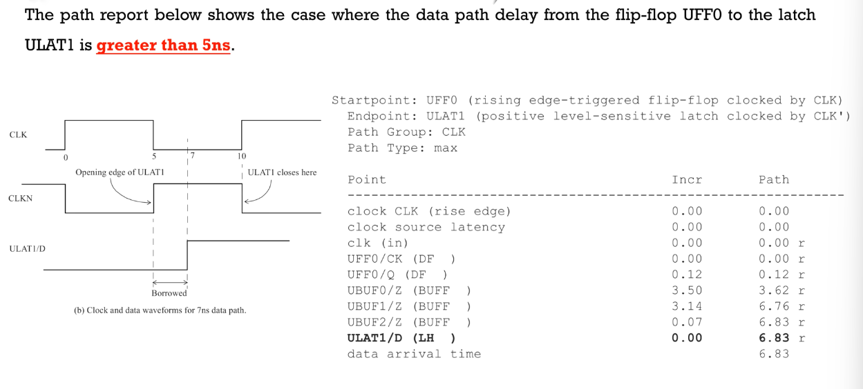
Graph & Wave
Here is an example of time borrowing using an active rising edge.
If data DIN is ready at time A prior to the latch opening on the rising edge of CLK at 10ns, the data flows to the output of the latch
as it opens.If data arrives at time B as shown for DIN (delayed), it borrows time Tb. However, this reduces the time available from the latch to the next flip-flop UFF2 - instead of a complete clock cycle, only time Ta is available.
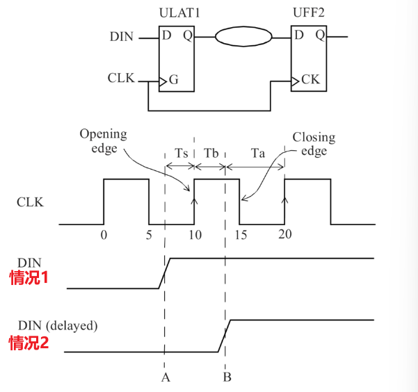
- 情况1:数据来的早,采样边沿前已经就绪
- 情况2:数据来的晚,采样边沿后还未就绪
positive slack, zero slack, and negative slack
- 有效点落在Ps,Zs,Ns
- 最多借半个周期
The timing regions for data arrival for positive slack, zero slack, and negative slack (that is, when a violation occurs)
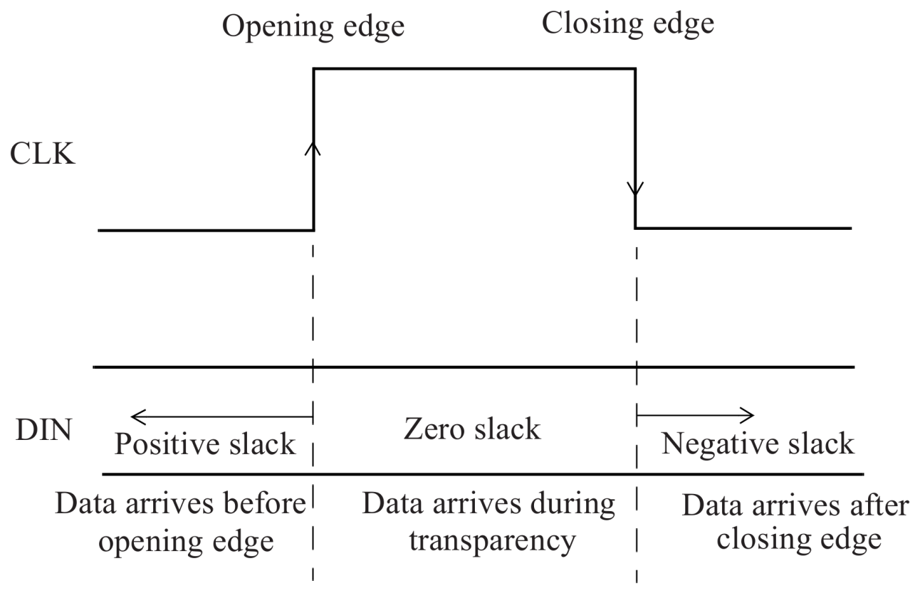
- Positive slave
- Zero slave
- Negative slave在Closing edge 后,时序违例,不正确(A data signal that arrives after the closing edge at the latch is a timing violation. )
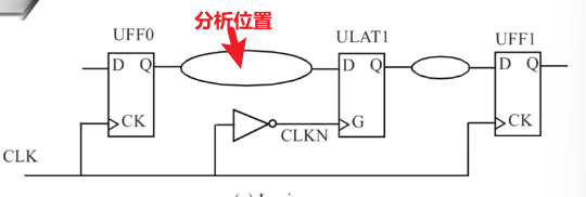
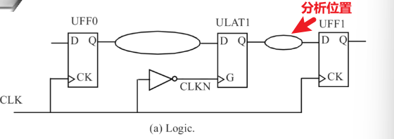
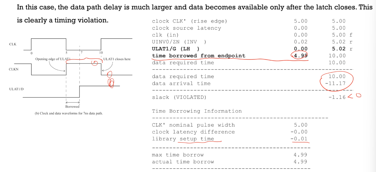
2)示例分析
This is the use of a latch with a half-cycle path to the next stage flip-flop.
We next describe three sets of timing reports for the latch example of it to illustrate the differen amounts of time borrowed from the next stage
一种clock gating门控时钟的电路示意图
This is the use of a latch with a half-cycle path to the next stage flip-flop.
We next describe three sets of timing reports for the latch example of it to illustrate the different amounts of time borrowed from the next stage
- Latch前接了个反相器,时钟端低电平有效
- 这种设计对于门控时钟可以消除毛刺
Positive slack
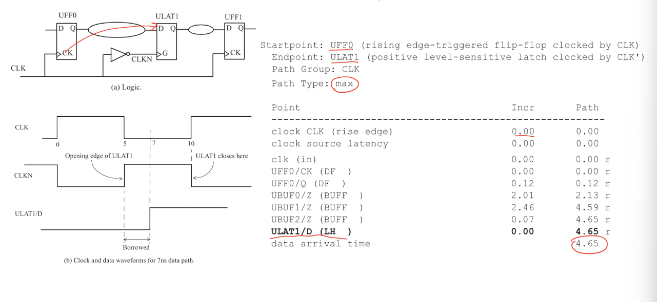
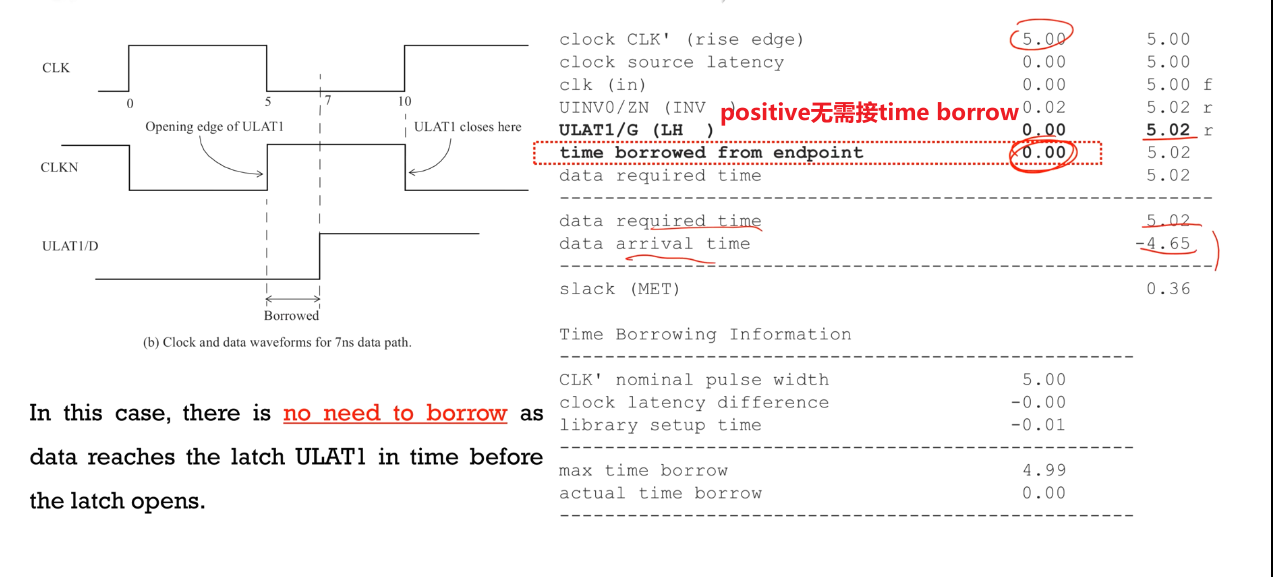
Zero slack
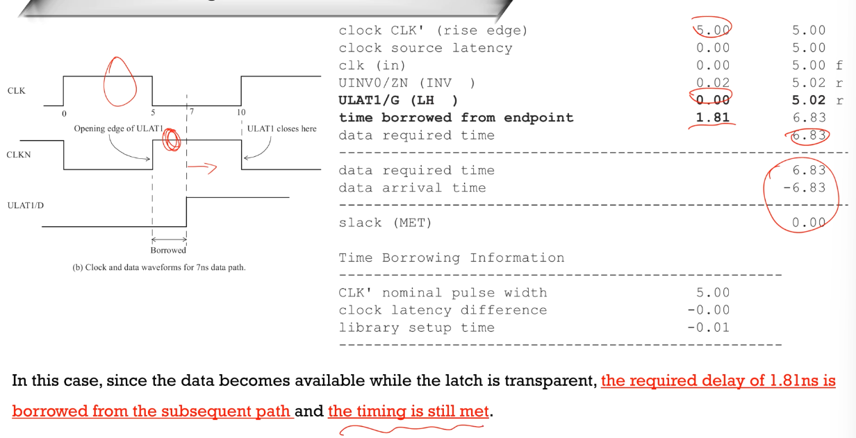

Zero slark后的时序路径分析
- 与前面zero slark相反
- 与半周期分析时类似
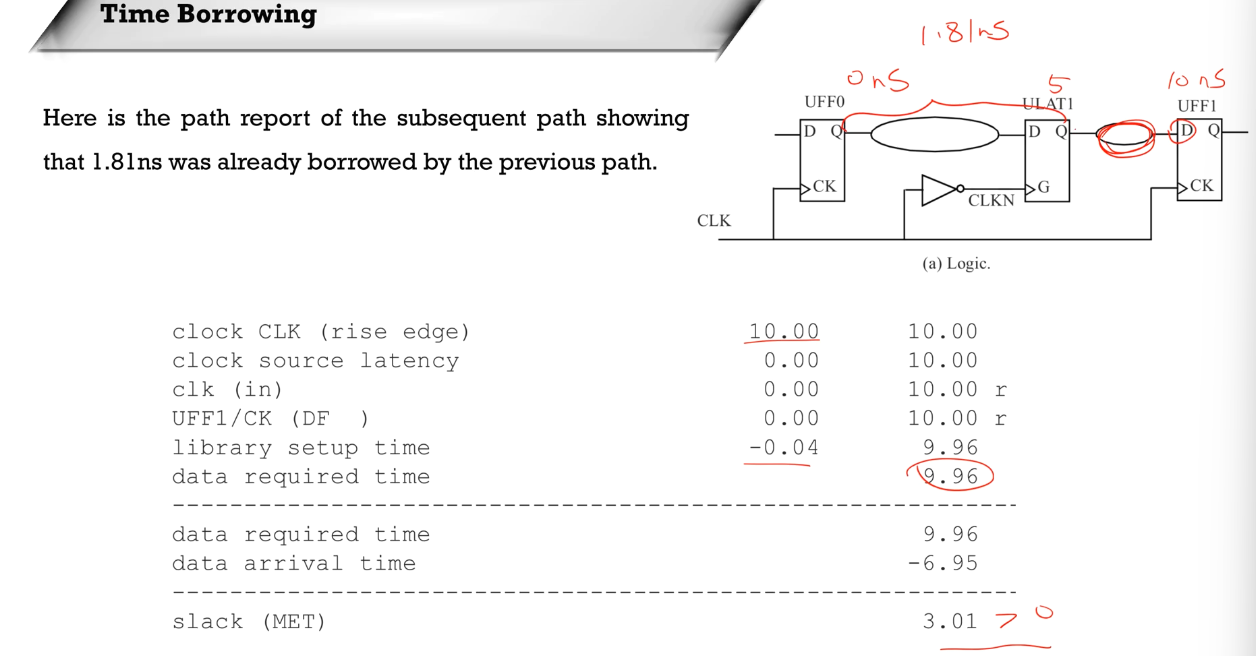
- 虽然前面借了0.81ns,总体看还是满足的
Negative slark
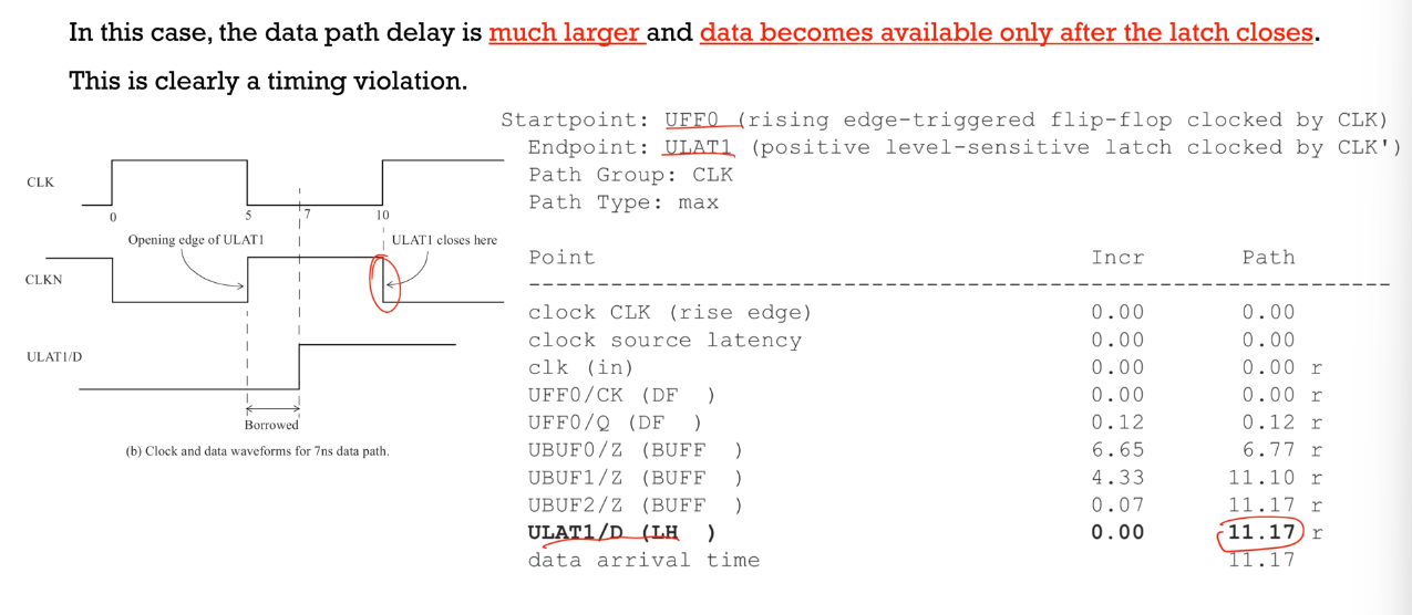
最多借半个周期
12 Data to Data Checks
12.1 概述
两个pins
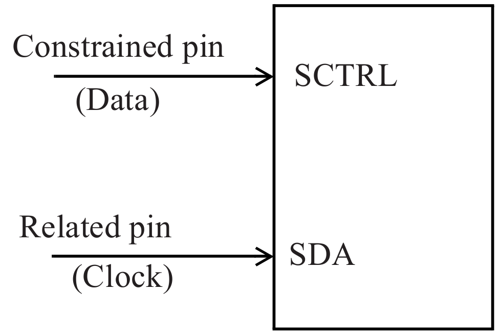
检查两个Pin之间的数据,且这两个Pin之间没有clock,这种时候我们通常把这两个Pin分为:
- Constrained pin:One pin is the constrained pin, which acts like a data pin of a flip-flop
- 看作D触发器的数据引脚
- Related pin:The second pin is the related pin, which acts like a clock pin of a flip-flop.
- 看作D触发器的时钟引脚
- 通过定义这两个pin来检查相对的时序约束
与ffcheck的不同
- The data to data setup check is performed on the same edge as the launch edge
- setup check的launch和capture在同一边沿(launch边沿)
- Unlike a normal setup check of a flip-flop, where the capture clock edge is normally one cycle away from the launch clock edge
- setup check的launch和capture在同一边沿,所以中间没有时钟,因此data to data checks也叫zero-cycle checks或same-cycle checks
12.2 如何实现data to data checks
基本模型
约束代码
1 | |
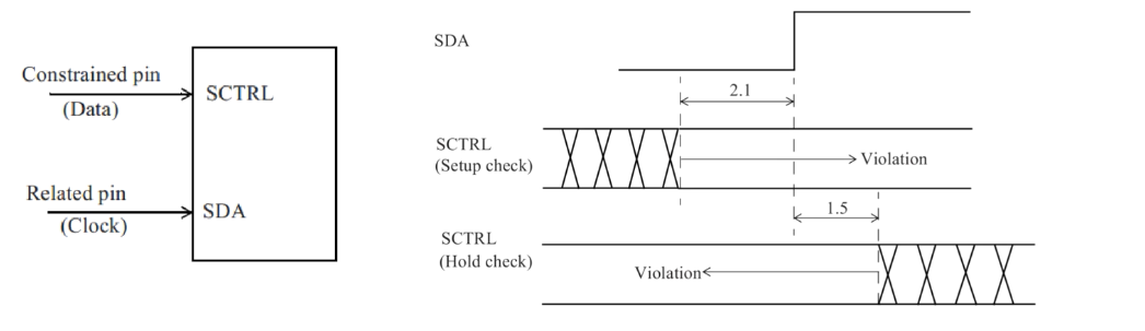
- The setup data check implies that SCTRL should arrive at least 2.1ns prior to the edge of the related pin SDA. Otherwise it is a data to data setup check violation.
The hold data check specifies that SCTRL should arrive at least 1.5ns after SDA. If the constraine signal arrives earlier than this specification, then it is a data to data hold check violation
This check is useful in a custom-designed block where it may be necessary to provide specific arrival times of one signal with respect to another.
- One such common situation is that of a data signal gated by an enable signal and it is required to
ensure that the enable signal is stable when the data signal arrives.
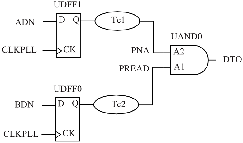
典型与门例子
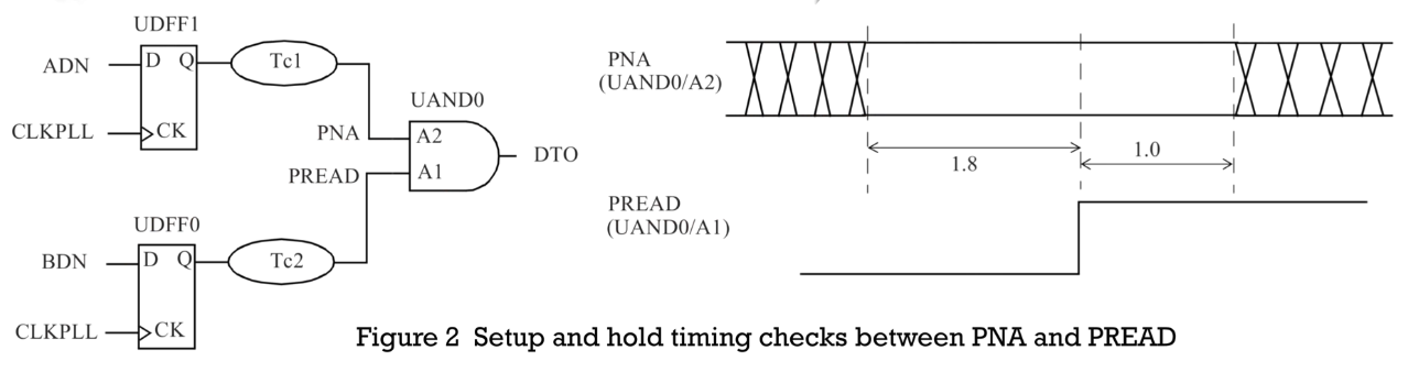
对于与门来说,数据必须非常稳定,否则会产生毛刺
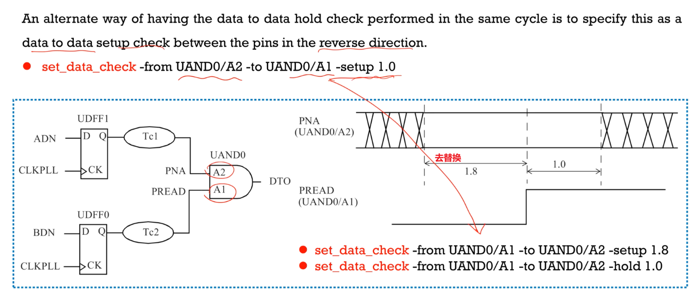
Consider the and cell shown in Figure 2. The requirement is to ensure that PNA arrives 1.8ns before the rising edge of PREAD and that it should not change for 1.0ns after the rising edge of PREAD. In this example, PNA is the constrained pin and PREAD is the related pin.
约束代码
1 | |
Report

- 这个report不满足要求,因此需要对电路进行优化
- 另外一个重要的点:One important aspect of a data to data setup check is that the clock edges that launch both the constrained pin and the related pin are from the same clock cycle (also referred to as same-cycle checks). Thus notice in the report that the starting time for the capture edge (UDFF0/CK) is at 0ns, not one cycle later as one would typically see in a setup report.
12.3 data to data hold check
默认的hold check往前一个周期
The zero-cycle setup check causes the hold timing check to be different from other hold check reports - the hold check is no longer on the same clock edge.
Here is the clock specification for CLKPLL which is utilized for the hold path report below
1 | |
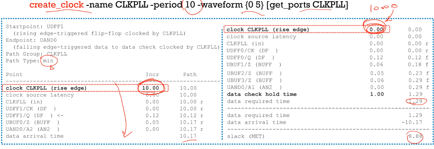
hold在同一周期的设置

In some scenarios, a designer may require the data to data hold check to be performed on the same clock cycle.
The same cycle hold requirement implies that the clock edge used for the related pin be moved back to where the clock edge for the constrained pin is.
This can be achieved by specifying a multicycle of -1:
1 | |

- 这里时序不满足(笑)
12.4 交换2pins
An alternate way of having the data to data hold check performed in the same cycle is to specify this as a data to data setup check between the pins in the reverse direction
1 | |
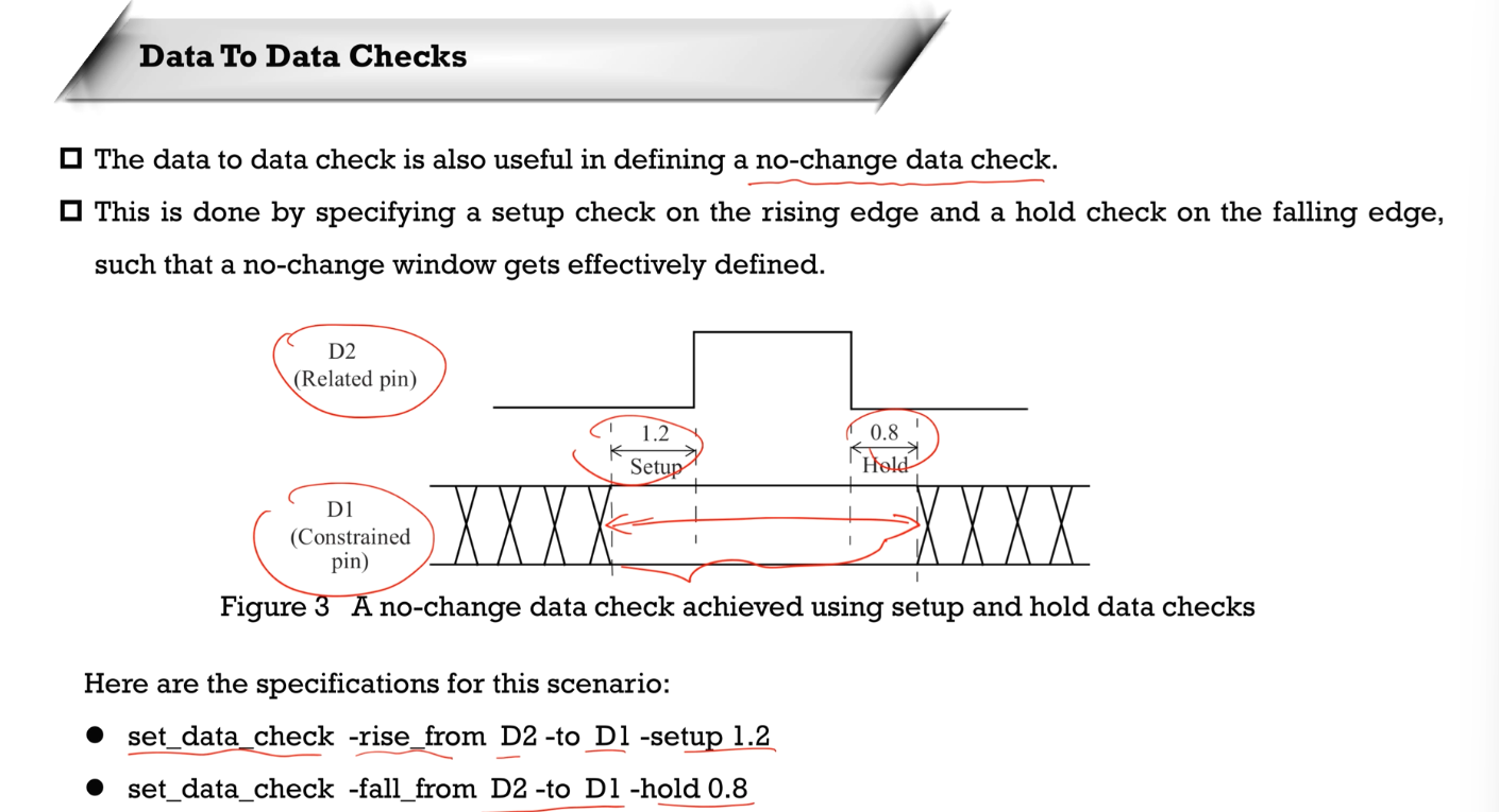
12.5 对无变化数据的检查
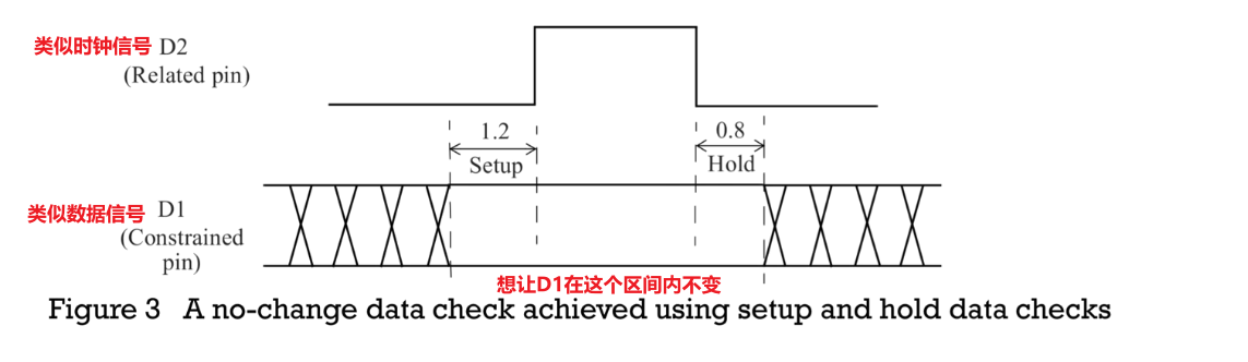
The data to data check is also useful in defining a no-change data check.
This is done by specifying a setup check on the rising edge and a hold check on the falling edge, such that a no-change window gets effectively defined
1 | |
13 习题讲解
本博客所有文章除特别声明外,均采用 CC BY-SA 4.0 协议 ,转载请注明出处!